M38507F8AFP#U1 Renesas Electronics America, M38507F8AFP#U1 Datasheet - Page 57
M38507F8AFP#U1
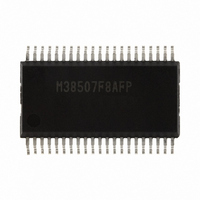
Manufacturer Part Number
M38507F8AFP#U1
Description
IC 740/3850 MCU FLASH 42SSOP
Manufacturer
Renesas Electronics America
Series
740/38000r
Datasheet
1.M38507F8AFPU1.pdf
(61 pages)
Specifications of M38507F8AFP#U1
Core Processor
740
Core Size
8-Bit
Speed
12.5MHz
Connectivity
SIO, UART/USART
Peripherals
PWM, WDT
Number Of I /o
32
Program Memory Size
32KB (32K x 8)
Program Memory Type
FLASH
Ram Size
1K x 8
Voltage - Supply (vcc/vdd)
1.8 V ~ 5.5 V
Data Converters
A/D 9x10b
Oscillator Type
Internal
Operating Temperature
-20°C ~ 85°C
Package / Case
42-SSOP
Package
42SSOP
Family Name
740
Maximum Speed
12.5 MHz
Operating Supply Voltage
5 V
Data Bus Width
8 Bit
Number Of Programmable I/os
34
Interface Type
UART
On-chip Adc
9-chx10-bit
Number Of Timers
4
Lead Free Status / RoHS Status
Lead free / RoHS Compliant
Eeprom Size
-
Available stocks
Company
Part Number
Manufacturer
Quantity
Price


3850 Group (Spec.A QzROM version)
Rev.2.13
REJ03B0125-0213
Notes on A/D Converter
1. Analog input pin
Make the signal source impedance for analog input low, or equip
an analog input pin with an external capacitor of 0.01
Further, be sure to verify the operation of application products on
the user side.
<Reason>
An analog input pin includes the capacitor for analog voltage
comparison. Accordingly, when signals from signal source with
high impedance are input to an analog input pin, charge and
discharge noise generates. This may cause the A/D conversion
precision to be worse.
2. A/D converter power source pin
The AV
using the A/D conversion function or not, connect it as following:
• AV
<Reason>
If the AV
because of noise or others.
3. Clock frequency during A/D conversion
The comparator consists of a capacity coupling, and a charge of
the capacity will be lost if the clock frequency is too low. Thus,
make sure the following during an A/D conversion.
• f(X
• Do not execute the STP instruction.
• When the A/D converter is operated at low-speed mode,
4. AD Input Selection Register
Be sure to fix bits 5 and 7 of the AD input selection register
(address 0037
Notes on Watchdog Timer
• Make sure that the watchdog timer does not underflow while
• When the STP instruction function selection bit has been set to
• The watchdog timer cannot be used in the middle-speed mode.
Notes on RESET Pin
1. Connecting capacitor
In case where the RESET signal rise time is long, connect a
ceramic capacitor or others across the RESET pin and the V
Use a 1000 pF or more capacitor for high frequency use. When
connecting the capacitor, note the following:
• Make the length of the wiring which is connected to a
• Be sure to verify the operation of application products on the
<Reason>
If the several nanosecond or several ten nanosecond impulse
noise enters the RESET pin, it may cause a microcomputer
failure.
f(X
A/D converter has a built-in self-oscillation circuit.
waiting Stop release, because the watchdog timer keeps
counting during that term.
“1”, it is impossible to switch it to “0” by a program.
(The internal reset may not be generated correctly, depending
on the underflow timing of the watchdog timer.)
capacitor as short as possible.
user side.
SS
IN
IN
: Connect to the V
) is 500 kHz or more in middle-/high-speed mode.
) do not have the lower limit of frequency, because of the
SS
SS
pin is A/D converter power source pin. Regardless of
pin is opened, the microcomputer may have a failure
16
Apr 17, 2009
) to “0”.
SS
line
Page 55 of 56
µ
F to 1
SS
pin.
µ
F.
2. Reset release after power on
When releasing the reset after power on, such as power-on reset,
release reset after X
where the power supply voltage is 1.8 V or more and the X
oscillation is stable.
<Reason>
To release reset, the RESET pin must be held at an “L” level for
20 cycles or more of X
voltage is between 1.8 V and 5.5 V, and X
Notes on Using Stop Mode
1. Register setting
Since values of the prescaler 12 and Timer 1 are automatically
reloaded when returning from the stop mode, set them again,
respectively. (When the oscillation stabilizing time set after STP
instruction released bit is “0”)
When using the oscillation stabilizing time set after STP
instruction released bit set to “1”, evaluate time to stabilize
oscillation of the used oscillator and set the value to the timer 1
and prescaler 12.
2. Clock restoration
After restoration from the stop mode to the normal mode by an
interrupt request, the contents of the CPU mode register previous
to the STP instruction execution are retained. Accordingly, if
both main clock and sub clock were oscillating before execution
of the STP instruction, the oscillation of both clocks is resumed
at restoration.
In the above case, when the main clock side is set as a system
clock, the oscillation stabilizing time for approximately 8,000
cycles of the X
mode. At this time, note that the oscillation on the sub clock side
may not be stabilized even after the lapse of the oscillation
stabilizing time of the main clock side.
Notes on Wait Mode
• Clock restoration
If the wait mode is released by a reset when X
system clock and X
the WIT instruction, X
starts, and X
In the above case, the RESET pin should be held at “L” until the
oscillation is stabilized.
Notes on Restarting Oscillation
• Restarting oscillation
Usually, when the MCU stops the clock oscillation by STP
instruction and the STP instruction has been released by an
external interrupt source, the fixed values of Timer 1 and
Prescaler 12 (Timer 1 = “01
automatically reloaded in order for the oscillation to stabilize.
The user can inhibit the automatic setting by writing “1” to bit 0
of MISRG (address 0038
However, by setting this bit to “1”, the previous values, set just
before the STP instruction was executed, will remain in Timer 1
and Prescaler 12. Therefore, you will need to set an appropriate
value to each register, in accordance with the oscillation
stabilizing time, before executing the STP instruction.
<Reason>
Oscillation will restart when an external interrupt is received.
However, internal clock
Timer 1 starts to underflow. This ensures time for the clock
oscillation using the ceramic resonators to be stabilized.
IN
is set as the system clock.
IN
input is reserved at restoration from the stop
IN
IN
oscillation is stopped during execution of
passes more than 20 cycles in the state
IN
CIN
16
φ
).
in the state where the power source
is supplied to the CPU only when
oscillation stops, X
16
”, Prescaler 12 = “FF
IN
oscillation is stable.
CIN
IN
is set as the
oscillations
16
”) are
IN
Related parts for M38507F8AFP#U1
Image
Part Number
Description
Manufacturer
Datasheet
Request
R

Part Number:
Description:
KIT STARTER FOR M16C/29
Manufacturer:
Renesas Electronics America
Datasheet:

Part Number:
Description:
KIT STARTER FOR R8C/2D
Manufacturer:
Renesas Electronics America
Datasheet:

Part Number:
Description:
R0K33062P STARTER KIT
Manufacturer:
Renesas Electronics America
Datasheet:

Part Number:
Description:
KIT STARTER FOR R8C/23 E8A
Manufacturer:
Renesas Electronics America
Datasheet:

Part Number:
Description:
KIT STARTER FOR R8C/25
Manufacturer:
Renesas Electronics America
Datasheet:

Part Number:
Description:
KIT STARTER H8S2456 SHARPE DSPLY
Manufacturer:
Renesas Electronics America
Datasheet:

Part Number:
Description:
KIT STARTER FOR R8C38C
Manufacturer:
Renesas Electronics America
Datasheet:

Part Number:
Description:
KIT STARTER FOR R8C35C
Manufacturer:
Renesas Electronics America
Datasheet:

Part Number:
Description:
KIT STARTER FOR R8CL3AC+LCD APPS
Manufacturer:
Renesas Electronics America
Datasheet:
Part Number:
Description:
KIT STARTER FOR RX610
Manufacturer:
Renesas Electronics America
Datasheet:

Part Number:
Description:
KIT STARTER FOR R32C/118
Manufacturer:
Renesas Electronics America
Datasheet:

Part Number:
Description:
KIT DEV RSK-R8C/26-29
Manufacturer:
Renesas Electronics America
Datasheet:

Part Number:
Description:
KIT STARTER FOR SH7124
Manufacturer:
Renesas Electronics America
Datasheet:

Part Number:
Description:
KIT STARTER FOR H8SX/1622
Manufacturer:
Renesas Electronics America
Datasheet:

Part Number:
Description:
KIT DEV FOR SH7203
Manufacturer:
Renesas Electronics America
Datasheet: