M38507F8AFP#U1 Renesas Electronics America, M38507F8AFP#U1 Datasheet - Page 55
M38507F8AFP#U1
Manufacturer Part Number
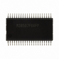
M38507F8AFP#U1
Description
IC 740/3850 MCU FLASH 42SSOP
Manufacturer
Renesas Electronics America
Series
740/38000r
Datasheet
1.M38507F8AFPU1.pdf
(61 pages)
Specifications of M38507F8AFP#U1
Core Processor
740
Core Size
8-Bit
Speed
12.5MHz
Connectivity
SIO, UART/USART
Peripherals
PWM, WDT
Number Of I /o
32
Program Memory Size
32KB (32K x 8)
Program Memory Type
FLASH
Ram Size
1K x 8
Voltage - Supply (vcc/vdd)
1.8 V ~ 5.5 V
Data Converters
A/D 9x10b
Oscillator Type
Internal
Operating Temperature
-20°C ~ 85°C
Package / Case
42-SSOP
Package
42SSOP
Family Name
740
Maximum Speed
12.5 MHz
Operating Supply Voltage
5 V
Data Bus Width
8 Bit
Number Of Programmable I/os
34
Interface Type
UART
On-chip Adc
9-chx10-bit
Number Of Timers
4
Lead Free Status / RoHS Status
Lead free / RoHS Compliant
Eeprom Size
-
Available stocks
Company
Part Number
Manufacturer
Quantity
Price


3850 Group (Spec.A QzROM version)
Rev.2.13
REJ03B0125-0213
Notes on Interrupts
1. Change of relevant register settings
When the setting of the following registers or bits is changed, the
interrupt request bit may be set to “1”. When not requiring the
interrupt occurrence synchronized with these setting, take the
following sequence.
• Interrupt edge selection register (address 003A
• Timer XY mode register (address 0023
Set the above listed registers or bits as the following sequence.
Fig 52. Sequence of changing relevant register
<Reason>
When setting the followings, the interrupt request bit may be set
to “1”.
• When setting external interrupt active edge
• When switching interrupt sources of an interrupt vector
2. Check of interrupt request bit
When executing the BBC or BBS instruction to an interrupt
request bit of an interrupt request register immediately after this bit
is set to “0” by using a data transfer instruction, execute one or
more instructions before executing the BBC or BBS instruction.
Fig 53. Sequence of check of interrupt request bit
<Reason>
If the BBC or BBS instruction is executed immediately after an
interrupt request bit of an interrupt request register is cleared to
“0”, the value of the interrupt request bit before being cleared to
“0” is read.
Concerned register:Interrupt edge selection register
address where two or more interrupt sources are allocated.
Concerned register: Interrupt edge selection register (address
003A
Set the corresponding interrupt enable bit to “0” (disabled).
Set the corresponding interrupt enable bit to “1” (enabled).
Set the interrupt edge select bit (active edge switch bit)
or the interrupt (source) select bit to “1”.
* Data transfer instruction:
Clear the interrupt request bit to “0” (no interrupt issued)
LDM, LDA, STA, STX, and STY instructions
16
Set the corresponding interrupt request bit to “0”
)
Apr 17, 2009
Execute the BBC or BBS instruction
NOP (one or more instructions)
NOP (one or more instructions)
(no interrupt request issued).
(address 003A
Timer XY mode register (address 0023
Page 53 of 56
16
)
16
)
16
)
16
)
3. Interrupt Request Register 1
Be sure to fix bits 1and 5 of the Interrupt request register 1
(address 003C
Notes on Timer
• If a value n (between 0 and 255) is written to a timer latch, the
• When switching the count source by the timer 12, X and Y
Notes on Serial Interface
1. Notes when selecting clock synchronous serial I/O
(1) Stop of transmission operation
Clear the serial I/O1 enable bit and the transmit enable bit to “0”
(Serial I/O1 and transmit disabled).
<Reason>
Since transmission is not stopped and the transmission circuit is
not initialized even if only the serial I/O1 enable bit is cleared to
“0” (Serial I/O1 disabled), the internal transmission is running
(in this case, since pins TxD, RxD, S
I/O ports, the transmission data is not output). When data is
written to the transmit buffer register in this state, data starts to
be shifted to the transmit shift register. When the serial I/O1
enable bit is set to “1” at this time, the data during internally
shifting is output to the TxD pin and an operation failure occurs.
(2) Stop of receive operation
Clear the receive enable bit to “0” (receive disabled), or clear the
serial I/O1 enable bit to “0” (Serial I/O1 disabled).
(3) Stop of transmit/receive operation
Clear the transmit enable bit and receive enable bit to “0”
simultaneously (transmit and receive disabled).
(when data is transmitted and received in the clock synchronous
serial I/O mode, any one of data transmission and reception
cannot be stopped.)
<Reason>
In the clock synchronous serial I/O mode, the same clock is used
for transmission and reception. If any one of transmission and
reception is disabled, a bit error occurs because transmission and
reception cannot be synchronized.
In this mode, the clock circuit of the transmission circuit also
operates for data reception. Accordingly, the transmission circuit
does not stop by clearing only the transmit enable bit to “0”
(transmit disabled). Also, the transmission circuit is not
initialized by clearing the serial I/O1 enable bit to “0” (Serial
I/O1 disabled) (refer to (1) in 1).
(4) S
When signals are output from the S
by using an external clock in the clock synchronous serial I/O
mode, set all of the receive enable bit, the S
bit, and the transmit enable bit to “1” (transmit enabled).
frequency division ratio is 1/(n+1).
count source selection bits, the value of timer count is altered
in unconsiderable amount owing to generating of thin pulses in
the count input signals.
Therefore, select the timer count source before set the value to
the prescaler and the timer.
(Serial I/O1)
RDY1
output of reception side (Serial I/O1)
16
) to “0”.
RDY1
CLK1
pin on the reception side
, and S
RDY1
RDY1
output enable
function as
Related parts for M38507F8AFP#U1
Image
Part Number
Description
Manufacturer
Datasheet
Request
R

Part Number:
Description:
KIT STARTER FOR M16C/29
Manufacturer:
Renesas Electronics America
Datasheet:

Part Number:
Description:
KIT STARTER FOR R8C/2D
Manufacturer:
Renesas Electronics America
Datasheet:

Part Number:
Description:
R0K33062P STARTER KIT
Manufacturer:
Renesas Electronics America
Datasheet:

Part Number:
Description:
KIT STARTER FOR R8C/23 E8A
Manufacturer:
Renesas Electronics America
Datasheet:

Part Number:
Description:
KIT STARTER FOR R8C/25
Manufacturer:
Renesas Electronics America
Datasheet:

Part Number:
Description:
KIT STARTER H8S2456 SHARPE DSPLY
Manufacturer:
Renesas Electronics America
Datasheet:

Part Number:
Description:
KIT STARTER FOR R8C38C
Manufacturer:
Renesas Electronics America
Datasheet:

Part Number:
Description:
KIT STARTER FOR R8C35C
Manufacturer:
Renesas Electronics America
Datasheet:

Part Number:
Description:
KIT STARTER FOR R8CL3AC+LCD APPS
Manufacturer:
Renesas Electronics America
Datasheet:
Part Number:
Description:
KIT STARTER FOR RX610
Manufacturer:
Renesas Electronics America
Datasheet:

Part Number:
Description:
KIT STARTER FOR R32C/118
Manufacturer:
Renesas Electronics America
Datasheet:

Part Number:
Description:
KIT DEV RSK-R8C/26-29
Manufacturer:
Renesas Electronics America
Datasheet:

Part Number:
Description:
KIT STARTER FOR SH7124
Manufacturer:
Renesas Electronics America
Datasheet:

Part Number:
Description:
KIT STARTER FOR H8SX/1622
Manufacturer:
Renesas Electronics America
Datasheet:

Part Number:
Description:
KIT DEV FOR SH7203
Manufacturer:
Renesas Electronics America
Datasheet: