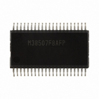
M38507F8AFP#U1 Renesas Electronics America, M38507F8AFP#U1 Datasheet - Page 35

M38507F8AFP#U1
Manufacturer Part Number
M38507F8AFP#U1
Description
IC 740/3850 MCU FLASH 42SSOP
Manufacturer
Renesas Electronics America
Series
740/38000r
Datasheet
1.M38507F8AFPU1.pdf
(61 pages)
Specifications of M38507F8AFP#U1
Core Processor
740
Core Size
8-Bit
Speed
12.5MHz
Connectivity
SIO, UART/USART
Peripherals
PWM, WDT
Number Of I /o
32
Program Memory Size
32KB (32K x 8)
Program Memory Type
FLASH
Ram Size
1K x 8
Voltage - Supply (vcc/vdd)
1.8 V ~ 5.5 V
Data Converters
A/D 9x10b
Oscillator Type
Internal
Operating Temperature
-20°C ~ 85°C
Package / Case
42-SSOP
Package
42SSOP
Family Name
740
Maximum Speed
12.5 MHz
Operating Supply Voltage
5 V
Data Bus Width
8 Bit
Number Of Programmable I/os
34
Interface Type
UART
On-chip Adc
9-chx10-bit
Number Of Timers
4
Lead Free Status / RoHS Status
Lead free / RoHS Compliant
Eeprom Size
-
Available stocks
Company
Part Number
Manufacturer
Quantity
Price
3850 Group (Spec.A QzROM version)
Rev.2.13
REJ03B0125-0213
A/D CONVERTER
[AD Conversion Registers (ADL, ADH)] 0035
The AD conversion registers are read-only registers that store the
result of an A/D conversion. Do not read these registers during
an A/D conversion.
[AD Control Register (ADCON)] 0034
The AD control register controls the A/D conversion process.
Bits 0 to 2 select a specific analog input pin. By setting a value to
these bits, when bit 0 of the AD input selection register (address
0037
0 of the AD input selection register is “1”, P0
be selected.
Bit 4 indicates the completion of an A/D conversion. The value
of this bit remains at “0” during an A/D conversion and changes
to “1” when an A/D conversion ends. Writing “0” to this bit starts
the A/D conversion.
[AD Input Selection Register (ADSEL)] 0037
The analog input port selection switch bit is assigned to bit 0 of
the AD input selection register. When “0” is set to the analog
input port selection switch bit, P3
by the analog input pin selection bits (b2, b1, b0) of the AD
control register (address 0034
input port selection switch bit, P0
by the analog input pin selection bits (b2, b1, b0) of the AD
control register (address 0034
• Comparison Voltage Generator
The comparison voltage generator divides the voltage between
AV
• Channel Selector
The channel selector selects one of ports P3
P0
• Comparator and Control Circuit
The comparator and control circuit compare an analog input
voltage with the comparison voltage, and the result is stored in
the AD conversion registers. When an A/D conversion is
completed, the control circuit sets the AD conversion completion
bit and the AD interrupt request bit to “1”.
Note that because the comparator consists of a capacitor
coupling, set f(X
conversion.
When the A/D converter is operated at low-speed mode, f(X
and f(X
the A/D converter has a built-in self-oscillation circuit.
4
SS
/AN
16
and V
) is “0”, P3
CIN
5
to P0
) do not have the lower limit of frequency, because of
REF
Apr 17, 2009
7
/AN
into 1024 and outputs the divided voltages.
0
/AN
8
IN
and inputs the voltage to the comparator.
) to 500 kHz or more during an A/D
0
-P3
4
/AN
16
16
).
). When “1” is set to the analog
0
4
4
Page 33 of 56
/AN
/AN
can be selected, and when bit
0
5
-P3
-P0
4
7
16
/AN
/AN
4
0
/AN
/AN
4
8
can be selected
can be selected
5
0
-P0
16
16
to P3
, 0036
7
/AN
4
/AN
8
16
can
IN
4
)
,
Fig 33. Structure of AD control register
Fig 34. Structure of AD input selection register
Fig 35. Structure of AD conversion registers
b7
b7
Notes 1: This is selected when bit 0 of the AD input selection register
8-bit reading (Read only address 0035
(Address 0035
10-bit reading
(Read address 0036
(Address 0036
(Address 0035
Note : The high-order 6 bits of address 0036
2: This is selected when bit 0 of the AD input selection register
at reading.
(address 0037
(address 0037
16
16
16
16
16
) is “0”.
) is “1”.
b0
)
)
)
b0
Analog input port selection switch bit
Not used (returns “0” when read)
Fix this bit to “0”.
Not used (returns “0” when read)
Fix this bit to “0”.
AD input selection register
(ADSEL: address 0037
0: P3
1: P0
16
b7
b9
b7
b7
b7
AD control register
(ADCON : address 0034
Analog input pin selection bits
Not used (returns “0” when read)
AD conversion completion bit
Not used (returns “0” when read)
b2 b1 b0
analog input pin.
analog input pin.
0 0 0: P3
0 0 1: P3
0 1 0: P3
0 1 1: P3
1 0 0: P3
0: Conversion in progress
1: Conversion completed
before 0035
0
4
b8 b7 b6 b5 b4 b3 b2
b6 b5 b4 b3 b2 b1 b0
/AN
/AN
0
5
to P3
to P0
0
1
2
3
4
Note 1
/AN
/AN
/AN
/AN
/AN
4
7
/AN
/AN
16
0 or
1 or
2 or
3 or
4
16
become “0”
4
8
16
is selected as
is selected as
)
)
P0
P0
P0
P0
b9 b8
16
16
4
5
6
7
)
Note 2
/AN
/AN
/AN
/AN
b0
b0
b0
)
5
6
7
8


