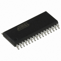
AT90PWM3-16SQ Atmel, AT90PWM3-16SQ Datasheet - Page 184

AT90PWM3-16SQ
Manufacturer Part Number
AT90PWM3-16SQ
Description
IC AVR MCU FLASH 8K 32SOIC
Manufacturer
Atmel
Series
AVR® 90PWM Lightingr
Datasheet
1.AT90PWM3B-16SU.pdf
(361 pages)
Specifications of AT90PWM3-16SQ
Core Processor
AVR
Core Size
8-Bit
Speed
16MHz
Connectivity
SPI, UART/USART
Peripherals
Brown-out Detect/Reset, POR, PWM, WDT
Number Of I /o
27
Program Memory Size
8KB (8K x 8)
Program Memory Type
FLASH
Eeprom Size
512 x 8
Ram Size
512 x 8
Voltage - Supply (vcc/vdd)
2.7 V ~ 5.5 V
Data Converters
A/D 11x10b; D/A 1x10b
Oscillator Type
Internal
Operating Temperature
-40°C ~ 105°C
Package / Case
32-SOIC (7.5mm Width)
Processor Series
AT90PWMx
Core
AVR8
Data Bus Width
8 bit
Data Ram Size
512 B
Interface Type
SPI, USART
Maximum Clock Frequency
16 MHz
Number Of Programmable I/os
27
Number Of Timers
2
Operating Supply Voltage
2.7 V to 5.5 V
Maximum Operating Temperature
+ 105 C
Mounting Style
SMD/SMT
3rd Party Development Tools
EWAVR, EWAVR-BL
Development Tools By Supplier
ATAVRDRAGON, ATSTK500, ATSTK600, ATAVRISP2, ATAVRONEKIT, ATAVRFBKIT, ATAVRISP2
Minimum Operating Temperature
- 40 C
On-chip Adc
10 bit, 11 Channel
On-chip Dac
10 bit, 1 Channel
For Use With
ATSTK600-SOIC - STK600 SOCKET/ADAPTER FOR SOICATAVRMC200 - KIT EVAL FOR AT90PWM3 ASYNCATAVRFBKIT - KIT DEMO BALLAST FOR AT90PWM2ATSTK520 - ADAPTER KIT FOR 90PWM
Lead Free Status / RoHS Status
Lead free / RoHS Compliant
- Current page: 184 of 361
- Download datasheet (7Mb)
18.3
184
Clock Generation
AT90PWM2/3/2B/3B
Figure 18-1. USART Block Diagram
Note:
The dashed boxes in the block diagram separate the three main parts of the USART (listed from
the top): Clock Generator, Transmitter and Receiver. Control registers are shared by all units.
The Clock Generation logic consists of synchronization logic for external clock input used by
synchronous slave operation, and the baud rate generator. The XCK (Transfer Clock) pin is only
used by synchronous transfer mode. The Transmitter consists of a single write buffer, a serial
Shift Register, Parity Generator and Control logic for handling different serial frame formats. The
write buffer allows a continuous transfer of data without any delay between frames. The
Receiver is the most complex part of the USART module due to its clock and data recovery
units. The recovery units are used for asynchronous data reception. In addition to the recovery
units, the Receiver includes a Parity Checker, Control logic, a Shift Register and a two level
receive buffer (UDR). The Receiver supports the same frame formats as the Transmitter, and
can detect Frame Error, Data OverRun and Parity Errors.
The Clock Generation logic generates the base clock for the Transmitter and Receiver. The
USART supports four modes of clock operation: Normal asynchronous, Double Speed asyn-
1. Refer to
pin placement.
Pin
Configurations3,
UCSRA
TRANSMIT SHIFT REGISTER
RECEIVE SHIFT REGISTER
BAUD RATE GENERATOR
UDR (Receive)
UDR (Transmit)
UBRR[H:L]
(1)
Table 11-9 on page
UCSRB
73, and
SYNC LOGIC
GENERATOR
RECOVERY
RECOVERY
CHECKER
PARITY
CLOCK
PARITY
DATA
CLKio
Table 11-7 on page 72
Clock Generator
CONTROL
CONTROL
CONTROL
CONTROL
CONTROL
Transmitter
PIN
PIN
PIN
RX
TX
Receiver
UCSRC
4317J–AVR–08/10
for USART
XCK
TxD
RxD
Related parts for AT90PWM3-16SQ
Image
Part Number
Description
Manufacturer
Datasheet
Request
R

Part Number:
Description:
IC AVR MCU FLASH 8K 32QFN
Manufacturer:
Atmel
Datasheet:

Part Number:
Description:
MCU AVR 8K FLASH 16MHZ 32-QFN
Manufacturer:
Atmel
Datasheet:

Part Number:
Description:
DEV KIT FOR AVR/AVR32
Manufacturer:
Atmel
Datasheet:

Part Number:
Description:
INTERVAL AND WIPE/WASH WIPER CONTROL IC WITH DELAY
Manufacturer:
ATMEL Corporation
Datasheet:

Part Number:
Description:
Low-Voltage Voice-Switched IC for Hands-Free Operation
Manufacturer:
ATMEL Corporation
Datasheet:

Part Number:
Description:
MONOLITHIC INTEGRATED FEATUREPHONE CIRCUIT
Manufacturer:
ATMEL Corporation
Datasheet:

Part Number:
Description:
AM-FM Receiver IC U4255BM-M
Manufacturer:
ATMEL Corporation
Datasheet:

Part Number:
Description:
Monolithic Integrated Feature Phone Circuit
Manufacturer:
ATMEL Corporation
Datasheet:

Part Number:
Description:
Multistandard Video-IF and Quasi Parallel Sound Processing
Manufacturer:
ATMEL Corporation
Datasheet:

Part Number:
Description:
High-performance EE PLD
Manufacturer:
ATMEL Corporation
Datasheet:

Part Number:
Description:
8-bit Flash Microcontroller
Manufacturer:
ATMEL Corporation
Datasheet:

Part Number:
Description:
2-Wire Serial EEPROM
Manufacturer:
ATMEL Corporation
Datasheet:


