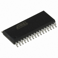
AT90PWM3-16SQ Atmel, AT90PWM3-16SQ Datasheet - Page 252

AT90PWM3-16SQ
Manufacturer Part Number
AT90PWM3-16SQ
Description
IC AVR MCU FLASH 8K 32SOIC
Manufacturer
Atmel
Series
AVR® 90PWM Lightingr
Datasheet
1.AT90PWM3B-16SU.pdf
(361 pages)
Specifications of AT90PWM3-16SQ
Core Processor
AVR
Core Size
8-Bit
Speed
16MHz
Connectivity
SPI, UART/USART
Peripherals
Brown-out Detect/Reset, POR, PWM, WDT
Number Of I /o
27
Program Memory Size
8KB (8K x 8)
Program Memory Type
FLASH
Eeprom Size
512 x 8
Ram Size
512 x 8
Voltage - Supply (vcc/vdd)
2.7 V ~ 5.5 V
Data Converters
A/D 11x10b; D/A 1x10b
Oscillator Type
Internal
Operating Temperature
-40°C ~ 105°C
Package / Case
32-SOIC (7.5mm Width)
Processor Series
AT90PWMx
Core
AVR8
Data Bus Width
8 bit
Data Ram Size
512 B
Interface Type
SPI, USART
Maximum Clock Frequency
16 MHz
Number Of Programmable I/os
27
Number Of Timers
2
Operating Supply Voltage
2.7 V to 5.5 V
Maximum Operating Temperature
+ 105 C
Mounting Style
SMD/SMT
3rd Party Development Tools
EWAVR, EWAVR-BL
Development Tools By Supplier
ATAVRDRAGON, ATSTK500, ATSTK600, ATAVRISP2, ATAVRONEKIT, ATAVRFBKIT, ATAVRISP2
Minimum Operating Temperature
- 40 C
On-chip Adc
10 bit, 11 Channel
On-chip Dac
10 bit, 1 Channel
For Use With
ATSTK600-SOIC - STK600 SOCKET/ADAPTER FOR SOICATAVRMC200 - KIT EVAL FOR AT90PWM3 ASYNCATAVRFBKIT - KIT DEMO BALLAST FOR AT90PWM2ATSTK520 - ADAPTER KIT FOR 90PWM
Lead Free Status / RoHS Status
Lead free / RoHS Compliant
- Current page: 252 of 361
- Download datasheet (7Mb)
AT90PWM2B/3B:
252
AT90PWM2/3/2B/3B
Until the conversion is not achieved, it is not possible to start a conversion on another channel.
In order to have a better understanding of the functioning of the amplifier synchronization, a tim-
ing diagram example is shown
Figure 21-15. Amplifier synchronization timing diagram for AT90PWM2/3.
It is also possible to auto trigger conversion on the amplified channel. In this case, the conver-
sion is started at the next amplifier clock event following the last auto trigger event selected
thanks to the ADTS bits in the ADCSRB register. In auto trigger conversion, the free running
mode is not possible unless the ADSC bit in ADCSRA is set by soft after each conversion.
Only PSC sources can auto trigger the amplified conversion. In this case, the core must have a
clock synchronous with the PSC. If the PSC uses the PLL clock, the core must use the PLL/4
clock source.
On PWM2B/3B, the amplifier has been improved in order to speed-up the conversion time.The
proposed improvement takes advantage of the amplifier characteristics to ensure a conversion
in less time.
In order to have a better understanding of the functioning of the amplifier synchronization, a tim-
ing diagram example is shown
Amplifier
Block
Block
ADC
PSC
Amplifier Sample
Amplifier Hold
(Sync Clock)
Signal to be
PSCn_ASY
AMPLI_clk
measured
ADASCR
CK ADC
Enable
ADSC
Value
Figure 21-15
Figure
for AT90PWM2B/3B.
Delta V
for AT90PWM2/3.
4th stable sample
Sampling
ADC Result Ready
ADC
Valid sample
4317J–AVR–08/10
Related parts for AT90PWM3-16SQ
Image
Part Number
Description
Manufacturer
Datasheet
Request
R

Part Number:
Description:
IC AVR MCU FLASH 8K 32QFN
Manufacturer:
Atmel
Datasheet:

Part Number:
Description:
MCU AVR 8K FLASH 16MHZ 32-QFN
Manufacturer:
Atmel
Datasheet:

Part Number:
Description:
DEV KIT FOR AVR/AVR32
Manufacturer:
Atmel
Datasheet:

Part Number:
Description:
INTERVAL AND WIPE/WASH WIPER CONTROL IC WITH DELAY
Manufacturer:
ATMEL Corporation
Datasheet:

Part Number:
Description:
Low-Voltage Voice-Switched IC for Hands-Free Operation
Manufacturer:
ATMEL Corporation
Datasheet:

Part Number:
Description:
MONOLITHIC INTEGRATED FEATUREPHONE CIRCUIT
Manufacturer:
ATMEL Corporation
Datasheet:

Part Number:
Description:
AM-FM Receiver IC U4255BM-M
Manufacturer:
ATMEL Corporation
Datasheet:

Part Number:
Description:
Monolithic Integrated Feature Phone Circuit
Manufacturer:
ATMEL Corporation
Datasheet:

Part Number:
Description:
Multistandard Video-IF and Quasi Parallel Sound Processing
Manufacturer:
ATMEL Corporation
Datasheet:

Part Number:
Description:
High-performance EE PLD
Manufacturer:
ATMEL Corporation
Datasheet:

Part Number:
Description:
8-bit Flash Microcontroller
Manufacturer:
ATMEL Corporation
Datasheet:

Part Number:
Description:
2-Wire Serial EEPROM
Manufacturer:
ATMEL Corporation
Datasheet:


