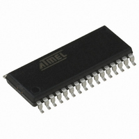
AT90PWM3-16SQ Atmel, AT90PWM3-16SQ Datasheet - Page 246

AT90PWM3-16SQ
Manufacturer Part Number
AT90PWM3-16SQ
Description
IC AVR MCU FLASH 8K 32SOIC
Manufacturer
Atmel
Series
AVR® 90PWM Lightingr
Datasheet
1.AT90PWM3B-16SU.pdf
(361 pages)
Specifications of AT90PWM3-16SQ
Core Processor
AVR
Core Size
8-Bit
Speed
16MHz
Connectivity
SPI, UART/USART
Peripherals
Brown-out Detect/Reset, POR, PWM, WDT
Number Of I /o
27
Program Memory Size
8KB (8K x 8)
Program Memory Type
FLASH
Eeprom Size
512 x 8
Ram Size
512 x 8
Voltage - Supply (vcc/vdd)
2.7 V ~ 5.5 V
Data Converters
A/D 11x10b; D/A 1x10b
Oscillator Type
Internal
Operating Temperature
-40°C ~ 105°C
Package / Case
32-SOIC (7.5mm Width)
Processor Series
AT90PWMx
Core
AVR8
Data Bus Width
8 bit
Data Ram Size
512 B
Interface Type
SPI, USART
Maximum Clock Frequency
16 MHz
Number Of Programmable I/os
27
Number Of Timers
2
Operating Supply Voltage
2.7 V to 5.5 V
Maximum Operating Temperature
+ 105 C
Mounting Style
SMD/SMT
3rd Party Development Tools
EWAVR, EWAVR-BL
Development Tools By Supplier
ATAVRDRAGON, ATSTK500, ATSTK600, ATAVRISP2, ATAVRONEKIT, ATAVRFBKIT, ATAVRISP2
Minimum Operating Temperature
- 40 C
On-chip Adc
10 bit, 11 Channel
On-chip Dac
10 bit, 1 Channel
For Use With
ATSTK600-SOIC - STK600 SOCKET/ADAPTER FOR SOICATAVRMC200 - KIT EVAL FOR AT90PWM3 ASYNCATAVRFBKIT - KIT DEMO BALLAST FOR AT90PWM2ATSTK520 - ADAPTER KIT FOR 90PWM
Lead Free Status / RoHS Status
Lead free / RoHS Compliant
- Current page: 246 of 361
- Download datasheet (7Mb)
21.8
21.8.1
246
ADC Register Description
AT90PWM2/3/2B/3B
ADC Multiplexer Register – ADMUX
Example 2:
The ADC of the AT90PWM2/2B/3/3B is controlled through 3 different registers. The ADCSRA
and The ADCSRB registers which are the ADC Control and Status registers, and the ADMUX
which allows to select the Vref source and the channel to be converted.
The conversion result is stored on ADCH and ADCL register which contain respectively the most
significant bits and the less significant bits.
Bit
Read/Write
Initial Value
• Bit 7, 6 – REFS1, 0: ADC Vref Selection Bits
These 2 bits determine the voltage reference for the ADC.
The different setting are shown in
Table 21-3.
If these bits are changed during a conversion, the change will not take effect until this conversion
is complete (it means while the ADIF bit in ADCSRA register is set).
In case the internal Vref is selected, it is turned ON as soon as an analog feature needed it is
set.
• Bit 5 – ADLAR: ADC Left Adjust Result
Set this bit to left adjust the ADC result.
Clear it to right adjust the ADC result.
The ADLAR bit affects the configuration of the ADC result data registers. Changing this bit
affects the ADC data registers immediately regardless of any on going conversion. For a com-
plete description of this bit, see Section “ADC Result Data Registers – ADCH and ADCL”,
page 250.
REFS1
0
0
1
1
–
–
–
–
–
ADCL will thus read 0x00, and ADCH will read 0x9C.
Writing zero to ADLAR right adjusts the result: ADCL = 0x70, ADCH = 0x02.
ADMUX = 0xFB (ADC3 - ADC2, 1x gain, 2.56V reference, left adjusted result)
Voltage on ADC3 is 300 mV, voltage on ADC2 is 500 mV.
ADCR = 512 * 1 * (300 - 500) / 2560 = -41 = 0x029.
ADCL will thus read 0x40, and ADCH will read 0x0A.
Writing zero to ADLAR right adjusts the result: ADCL = 0x00, ADCH = 0x29.
ADC Voltage Reference Selection
REFS0
0
1
0
1
REFS1
R/W
7
0
REFS0
R/W
6
0
Description
External Vref on AREF pin, Internal Vref is switched off
AVcc with external capacitor connected on the AREF pin
Reserved
Internal 2.56V Reference voltage with external capacitor connected on
the AREF pin
ADLAR
Table
R/W
5
0
21-3.
4
0
-
-
MUX3
R/W
3
0
MUX2
R/W
2
0
MUX1
R/W
1
0
MUX0
R/W
0
0
4317J–AVR–08/10
ADMUX
Related parts for AT90PWM3-16SQ
Image
Part Number
Description
Manufacturer
Datasheet
Request
R

Part Number:
Description:
IC AVR MCU FLASH 8K 32QFN
Manufacturer:
Atmel
Datasheet:

Part Number:
Description:
MCU AVR 8K FLASH 16MHZ 32-QFN
Manufacturer:
Atmel
Datasheet:

Part Number:
Description:
DEV KIT FOR AVR/AVR32
Manufacturer:
Atmel
Datasheet:

Part Number:
Description:
INTERVAL AND WIPE/WASH WIPER CONTROL IC WITH DELAY
Manufacturer:
ATMEL Corporation
Datasheet:

Part Number:
Description:
Low-Voltage Voice-Switched IC for Hands-Free Operation
Manufacturer:
ATMEL Corporation
Datasheet:

Part Number:
Description:
MONOLITHIC INTEGRATED FEATUREPHONE CIRCUIT
Manufacturer:
ATMEL Corporation
Datasheet:

Part Number:
Description:
AM-FM Receiver IC U4255BM-M
Manufacturer:
ATMEL Corporation
Datasheet:

Part Number:
Description:
Monolithic Integrated Feature Phone Circuit
Manufacturer:
ATMEL Corporation
Datasheet:

Part Number:
Description:
Multistandard Video-IF and Quasi Parallel Sound Processing
Manufacturer:
ATMEL Corporation
Datasheet:

Part Number:
Description:
High-performance EE PLD
Manufacturer:
ATMEL Corporation
Datasheet:

Part Number:
Description:
8-bit Flash Microcontroller
Manufacturer:
ATMEL Corporation
Datasheet:

Part Number:
Description:
2-Wire Serial EEPROM
Manufacturer:
ATMEL Corporation
Datasheet:


