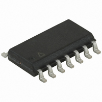
ATTINY24-15SSZ Atmel, ATTINY24-15SSZ Datasheet - Page 105

ATTINY24-15SSZ
Manufacturer Part Number
ATTINY24-15SSZ
Description
MCU AVR 2K FLASH 15MHZ 14-SOIC
Manufacturer
Atmel
Series
AVR® ATtinyr
Datasheet
1.ATTINY24-15SSZ.pdf
(225 pages)
Specifications of ATTINY24-15SSZ
Package / Case
14-SOIC (3.9mm Width), 14-SOL
Voltage - Supply (vcc/vdd)
2.7 V ~ 5.5 V
Operating Temperature
-40°C ~ 125°C
Speed
16MHz
Number Of I /o
12
Eeprom Size
128 x 8
Core Processor
AVR
Program Memory Type
FLASH
Ram Size
128 x 8
Program Memory Size
2KB (2K x 8)
Data Converters
A/D 8x10b
Oscillator Type
Internal
Peripherals
Brown-out Detect/Reset, POR, PWM, WDT
Connectivity
USI
Core Size
8-Bit
Cpu Family
ATtiny
Device Core
AVR
Device Core Size
8b
Frequency (max)
16MHz
Interface Type
SPI/UART
Total Internal Ram Size
128Byte
# I/os (max)
12
Number Of Timers - General Purpose
2
Operating Supply Voltage (typ)
3.3/5V
Operating Supply Voltage (max)
5.5V
Operating Supply Voltage (min)
2.7V
On-chip Adc
8-chx10-bit
Instruction Set Architecture
RISC
Operating Temp Range
-40C to 125C
Operating Temperature Classification
Automotive
Mounting
Surface Mount
Pin Count
14
Package Type
SOIC
Lead Free Status / RoHS Status
Lead free / RoHS Compliant
Available stocks
Company
Part Number
Manufacturer
Quantity
Price
Company:
Part Number:
ATTINY24-15SSZ
Manufacturer:
ATMEL
Quantity:
349
Part Number:
ATTINY24-15SSZ
Manufacturer:
ATTINY
Quantity:
20 000
7701D–AVR–09/10
When changing the top value, the program must ensure that the new top value is higher or
equal to the value of all of the compare registers. If the top value is lower than any of the com-
pare registers, a compare match will never occur between TCNT1 and OCR1x. Note that
when using fixed top values, the unused bits are masked to zero when any of the OCR1x Reg-
isters are written
The procedure for updating ICR1 differs from that for updating OCR1A when used for defining
the top value. The ICR1 register is not double buffered. This means that if ICR1 is changed to
a low value when the counter is running with no or a low prescaler value, there is a risk that the
new ICR1 value written is lower than the current value of TCNT1. The result will then be that
the counter will miss the compare match at the top value. The counter will then have to count
to the max value (0xFFFF) and wrap around starting at 0x0000 before the compare match can
occur. The OCR1A register, however, is double buffered. This feature allows the OCR1A I/O
location to be written anytime. When the OCR1A I/O location is written, the value written will
be put into the OCR1A buffer register. The OCR1A compare register will then be updated with
the value in the buffer register at the next timer clock cycle when TCNT1 matches top. The
update is done on the same timer clock cycle on which TCNT1 is cleared and the TOV1 flag is
set.
Using the ICR1 register for defining top works well when using fixed top values. By using
ICR1, the OCR1A register is free to be used for generating a PWM output on OC1A. How-
ever, if the base PWM frequency is actively changed (by changing the top value), using the
OCR1A as top is clearly a better choice due to its double buffer feature.
In fast PWM mode, the compare units allow generation of PWM waveforms on the OC1x pins.
Setting the COM1x1:0 bits to two will produce a non-inverted PWM, and an inverted PWM out-
put can be generated by setting the COM1x1:0 to three (see
actual OC1x value will only be visible on the port pin if the data direction for the port pin is set
as output (DDR_OC1x). The PWM waveform is generated by setting (or clearing) the OC1x
register at the compare match between OCR1x and TCNT1, and clearing (or setting) the
OC1x register on the timer clock cycle on which the counter is cleared (changes from top to
bottom).
The PWM frequency for the output can be calculated by the following equation:
The variable N represents the prescaler divider (1, 8, 64, 256, or 1024).
The extreme values for the OCR1x register represent special cases when generating a PWM
waveform output in the fast PWM mode. If the OCR1x is set equal to bottom (0x0000), the out-
put will be a narrow spike for each top+1 timer clock cycle. Setting OCR1x equal to top will
result in a constant high or low output (depending on the polarity of the output set by the
COM1x1:0 bits.)
A frequency waveform output (with 50% duty cycle) in fast PWM mode can be achieved by
setting OC1A to toggle its logical level on each compare match (COM1A1:0 = 1). The wave-
form generated will have a maximum frequency of
(0x0000). This feature is similar to the OC1A toggle in CTC mode, except the double buffer
feature of the output compare unit is enabled in the fast PWM mode.
f
OCnxPWM
=
-------------------------------------
N
f
clk_I/O
1
+
TOP
Atmel ATtiny24/44/84 [Preliminary]
1
A
= f
clk_I/O
/2 when OCR1A is set to zero
Table 14-2 on page
112). The
105


