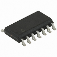
ATTINY24-15SSZ Atmel, ATTINY24-15SSZ Datasheet - Page 99

ATTINY24-15SSZ
Manufacturer Part Number
ATTINY24-15SSZ
Description
MCU AVR 2K FLASH 15MHZ 14-SOIC
Manufacturer
Atmel
Series
AVR® ATtinyr
Datasheet
1.ATTINY24-15SSZ.pdf
(225 pages)
Specifications of ATTINY24-15SSZ
Package / Case
14-SOIC (3.9mm Width), 14-SOL
Voltage - Supply (vcc/vdd)
2.7 V ~ 5.5 V
Operating Temperature
-40°C ~ 125°C
Speed
16MHz
Number Of I /o
12
Eeprom Size
128 x 8
Core Processor
AVR
Program Memory Type
FLASH
Ram Size
128 x 8
Program Memory Size
2KB (2K x 8)
Data Converters
A/D 8x10b
Oscillator Type
Internal
Peripherals
Brown-out Detect/Reset, POR, PWM, WDT
Connectivity
USI
Core Size
8-Bit
Cpu Family
ATtiny
Device Core
AVR
Device Core Size
8b
Frequency (max)
16MHz
Interface Type
SPI/UART
Total Internal Ram Size
128Byte
# I/os (max)
12
Number Of Timers - General Purpose
2
Operating Supply Voltage (typ)
3.3/5V
Operating Supply Voltage (max)
5.5V
Operating Supply Voltage (min)
2.7V
On-chip Adc
8-chx10-bit
Instruction Set Architecture
RISC
Operating Temp Range
-40C to 125C
Operating Temperature Classification
Automotive
Mounting
Surface Mount
Pin Count
14
Package Type
SOIC
Lead Free Status / RoHS Status
Lead free / RoHS Compliant
Available stocks
Company
Part Number
Manufacturer
Quantity
Price
Company:
Part Number:
ATTINY24-15SSZ
Manufacturer:
ATMEL
Quantity:
349
Part Number:
ATTINY24-15SSZ
Manufacturer:
ATTINY
Quantity:
20 000
- Current page: 99 of 225
- Download datasheet (4Mb)
14.7
7701D–AVR–09/10
Output Compare Units
Measurement of an external signal's duty cycle requires that the trigger edge be changed after
each capture. Changing the edge sensing must be done as early as possible after the ICR1
register has been read. After a change of the edge, the input capture flag (ICF1) must be
cleared by software (writing a logical one to the I/O bit location). For measuring frequency
only, the clearing of the ICF1 flag is not required (if an interrupt handler is used).
The 16-bit comparator continuously compares TCNT1 with the output compare register
(OCR1x). If TCNT equals OCR1x, the comparator signals a match. A match will set the output
compare flag (OCF1x) at the next timer clock cycle. If enabled (OCIE1x = 1), the output com-
pare flag generates an output compare interrupt. The OCF1x flag is automatically cleared
when the interrupt is executed. Alternatively the OCF1x flag can be cleared by software by
writing a logical one to its I/O bit location. The waveform generator uses the match signal to
generate an output according to the operating mode set by the waveform generation mode
(WGM13:0) bits and compare output mode (COM1x1:0) bits. The top and bottom signals are
used by the waveform generator for handling the special cases of the extreme values in some
modes of operation
A special feature of Output Compare unit A allows it to define the Timer/Counter TOP value
(i.e., counter resolution). In addition to the counter resolution, the TOP value defines the
period time for waveforms generated by the Waveform Generator.
Figure 14-4 on page 99
register and bit names indicates the device number (n = 1 for timer/counter 1), and the "x" indi-
cates output compare unit (A/B). The elements of the block diagram that are not directly a part
of the output compare unit are shaded gray.
Figure 14-4. Output Compare Unit, Block Diagram
(“Modes of Operation” on page
shows a block diagram of the output compare unit. The small "n" in the
OCRnxH Buf. (8-bit)
OCRnxH (8-bit)
Atmel ATtiny24/44/84 [Preliminary]
BOTTOM
OCRnx Buffer (16-bit Register)
TEMP (8-bit)
TOP
OCRnx (16-bit Register)
OCRnxL Buf. (8-bit)
OCRnxL (8-bit)
DATA BUS
Waveform Generator
WGMn3:0
=
(16-bit Comparator )
102).
(8-bit)
COMnx1:0
TCNTnH (8-bit)
OCFnx (Int.Req.)
TCNTn (16-bit Counter)
TCNTnL (8-bit)
OCnx
99
Related parts for ATTINY24-15SSZ
Image
Part Number
Description
Manufacturer
Datasheet
Request
R

Part Number:
Description:
Manufacturer:
Atmel Corporation
Datasheet:

Part Number:
Description:
Manufacturer:
Atmel Corporation
Datasheet:

Part Number:
Description:
IC MCU AVR 2K FLASH 20MHZ 20-QFN
Manufacturer:
Atmel
Datasheet:

Part Number:
Description:
IC MCU AVR 2K FLASH 20MHZ 14SOIC
Manufacturer:
Atmel
Datasheet:

Part Number:
Description:
MCU AVR 2K FLASH 15MHZ 20-QFN
Manufacturer:
Atmel
Datasheet:

Part Number:
Description:
IC MCU AVR 2K FLASH 20MHZ 14-DIP
Manufacturer:
Atmel
Datasheet:

Part Number:
Description:
MCU AVR 2KB FLASH 20MHZ 14SOIC
Manufacturer:
Atmel
Datasheet:

Part Number:
Description:
MCU AVR 2KB FLASH 20MHZ 20QFN
Manufacturer:
Atmel
Datasheet:

Part Number:
Description:
IC, MCU, 8BIT, 2K FLASH, 20SOIC
Manufacturer:
Atmel
Datasheet:

Part Number:
Description:
IC, MCU, 8BIT, 2K FLASH, 20PDIP
Manufacturer:
Atmel
Datasheet:

Part Number:
Description:
IC, MCU, 8BIT, 8K FLASH, 20PDIP
Manufacturer:
Atmel
Datasheet:

Part Number:
Description:
IC, MCU, 8BIT, 8K FLASH, 20SOIC
Manufacturer:
Atmel
Datasheet:


