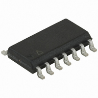
ATTINY24-15SSZ Atmel, ATTINY24-15SSZ Datasheet - Page 172

ATTINY24-15SSZ
Manufacturer Part Number
ATTINY24-15SSZ
Description
MCU AVR 2K FLASH 15MHZ 14-SOIC
Manufacturer
Atmel
Series
AVR® ATtinyr
Datasheet
1.ATTINY24-15SSZ.pdf
(225 pages)
Specifications of ATTINY24-15SSZ
Package / Case
14-SOIC (3.9mm Width), 14-SOL
Voltage - Supply (vcc/vdd)
2.7 V ~ 5.5 V
Operating Temperature
-40°C ~ 125°C
Speed
16MHz
Number Of I /o
12
Eeprom Size
128 x 8
Core Processor
AVR
Program Memory Type
FLASH
Ram Size
128 x 8
Program Memory Size
2KB (2K x 8)
Data Converters
A/D 8x10b
Oscillator Type
Internal
Peripherals
Brown-out Detect/Reset, POR, PWM, WDT
Connectivity
USI
Core Size
8-Bit
Cpu Family
ATtiny
Device Core
AVR
Device Core Size
8b
Frequency (max)
16MHz
Interface Type
SPI/UART
Total Internal Ram Size
128Byte
# I/os (max)
12
Number Of Timers - General Purpose
2
Operating Supply Voltage (typ)
3.3/5V
Operating Supply Voltage (max)
5.5V
Operating Supply Voltage (min)
2.7V
On-chip Adc
8-chx10-bit
Instruction Set Architecture
RISC
Operating Temp Range
-40C to 125C
Operating Temperature Classification
Automotive
Mounting
Surface Mount
Pin Count
14
Package Type
SOIC
Lead Free Status / RoHS Status
Lead free / RoHS Compliant
Available stocks
Company
Part Number
Manufacturer
Quantity
Price
Company:
Part Number:
ATTINY24-15SSZ
Manufacturer:
ATMEL
Quantity:
349
Part Number:
ATTINY24-15SSZ
Manufacturer:
ATTINY
Quantity:
20 000
- Current page: 172 of 225
- Download datasheet (4Mb)
21.8.3
21.8.4
172
Atmel ATtiny24/44/84 [Preliminary]
Chip Erase
Programming the Flash
The Chip Erase will erase the Flash and EEPROM
bits are not reset until the program memory has been completely erased. The fuse bits are not
changed. A chip erase must be performed before the flash and/or EEPROM are
reprogrammed.
Note:
1. Load "Chip Erase" command (see
2. Wait after Instr. 3 until SDO goes high for the “Chip Erase” cycle to finish.
3. Load "No Operation" command.
The Flash is organized in pages, see
the program data are latched into a page buffer. This allows one page of program data to be
programmed simultaneously. The following procedure describes how to program the entire
flash memory:
1. Load "Write Flash" command (see
2. Load Flash Page Buffer.
3. Load Flash High Address and Program Page. Wait after Instr. 3 until SDO goes high for
4. Repeat 2 and 3 until the entire flash is programmed, or until all data has been
5. End page programming by loading "No Operation" command.
When writing or reading serial data to the Atmel
ing edge of the serial clock. See
22-9 on page 185
Figure 21-4. Addressing the Flash which is Organized in Pages
the “Page Programming” cycle to finish.
programmed.
1. The EEPROM memory is preserved during Chip Erase if the EESAVE Fuse is programmed.
PROGRAM MEMORY
PROGRAM
COUNTER
PAGE
for details.
PAGE ADDRESS
WITHIN THE FLASH
PCMSB
PCPAGE
Figure 22-5 on page
“Page Size” on page
Table 21-15 on page
Table 21-15 on page
PAGEMSB
PCWORD
WORD ADDRESS
WITHIN A PAGE
®
ATtiny24/44/84, data are clocked on the ris-
(1)
185,
memories, as well as lock bits. The lock
INSTRUCTION WORD
Figure 21-3 on page 170
165. When programming the flash,
PAGE
174).
174).
PCWORD[PAGEMSB:0]:
00
01
02
PAGEEND
7701D–AVR–09/10
and
Table
Related parts for ATTINY24-15SSZ
Image
Part Number
Description
Manufacturer
Datasheet
Request
R

Part Number:
Description:
Manufacturer:
Atmel Corporation
Datasheet:

Part Number:
Description:
Manufacturer:
Atmel Corporation
Datasheet:

Part Number:
Description:
IC MCU AVR 2K FLASH 20MHZ 20-QFN
Manufacturer:
Atmel
Datasheet:

Part Number:
Description:
IC MCU AVR 2K FLASH 20MHZ 14SOIC
Manufacturer:
Atmel
Datasheet:

Part Number:
Description:
MCU AVR 2K FLASH 15MHZ 20-QFN
Manufacturer:
Atmel
Datasheet:

Part Number:
Description:
IC MCU AVR 2K FLASH 20MHZ 14-DIP
Manufacturer:
Atmel
Datasheet:

Part Number:
Description:
MCU AVR 2KB FLASH 20MHZ 14SOIC
Manufacturer:
Atmel
Datasheet:

Part Number:
Description:
MCU AVR 2KB FLASH 20MHZ 20QFN
Manufacturer:
Atmel
Datasheet:

Part Number:
Description:
IC, MCU, 8BIT, 2K FLASH, 20SOIC
Manufacturer:
Atmel
Datasheet:

Part Number:
Description:
IC, MCU, 8BIT, 2K FLASH, 20PDIP
Manufacturer:
Atmel
Datasheet:

Part Number:
Description:
IC, MCU, 8BIT, 8K FLASH, 20PDIP
Manufacturer:
Atmel
Datasheet:

Part Number:
Description:
IC, MCU, 8BIT, 8K FLASH, 20SOIC
Manufacturer:
Atmel
Datasheet:


