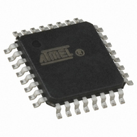
AT90USB162-16AU Atmel, AT90USB162-16AU Datasheet - Page 74

AT90USB162-16AU
Manufacturer Part Number
AT90USB162-16AU
Description
MCU AVR USB 16K FLASH 32-TQFP
Manufacturer
Atmel
Series
AVR® 90USBr
Datasheet
1.AT90USB82-16MU.pdf
(307 pages)
Specifications of AT90USB162-16AU
Core Processor
AVR
Core Size
8-Bit
Speed
16MHz
Connectivity
EBI/EMI, PS/2, SPI, UART/USART, USB
Peripherals
Brown-out Detect/Reset, POR, PWM, WDT
Number Of I /o
22
Program Memory Size
16KB (16K x 8)
Program Memory Type
FLASH
Eeprom Size
512 x 8
Ram Size
512 x 8
Voltage - Supply (vcc/vdd)
2.7 V ~ 5.5 V
Oscillator Type
Internal
Operating Temperature
-40°C ~ 85°C
Package / Case
32-TQFP, 32-VQFP
Processor Series
AT90USBx
Core
AVR8
Data Bus Width
8 bit
Data Ram Size
512 B
Interface Type
SPI/USART/debugWIRE
Maximum Clock Frequency
16 MHz
Number Of Programmable I/os
22
Number Of Timers
2
Operating Supply Voltage
2.7 V to 5.5 V
Maximum Operating Temperature
+ 85 C
Mounting Style
SMD/SMT
3rd Party Development Tools
EWAVR, EWAVR-BL
Development Tools By Supplier
ATAVRDRAGON, ATSTK500, ATSTK600, ATSTK525, ATSTK526, ATAVRISP2, ATAVRONEKIT, AT90USBKEY, ATEVK525
Minimum Operating Temperature
- 40 C
No. Of I/o's
22
Eeprom Memory Size
512Byte
Ram Memory Size
512Byte
Cpu Speed
16MHz
No. Of Timers
2
Embedded Interface Type
SPI, USART
Rohs Compliant
Yes
For Use With
ATSTK600 - DEV KIT FOR AVR/AVR32ATSTK526 - KIT STARTER FOR AT90USB82/162ATAVRDRAGON - KIT DRAGON 32KB FLASH MEM AVRATSTK525 - KIT STARTER FOR AT90USBAT90USBKEY2 - KIT DEMO FOR AT90USB
Lead Free Status / RoHS Status
Lead free / RoHS Compliant
Data Converters
-
Lead Free Status / Rohs Status
Lead free / RoHS Compliant
Available stocks
Company
Part Number
Manufacturer
Quantity
Price
Company:
Part Number:
AT90USB162-16AU
Manufacturer:
Atmel
Quantity:
30 024
Part Number:
AT90USB162-16AU
Manufacturer:
MICROCHIP/微芯
Quantity:
20 000
Company:
Part Number:
AT90USB162-16AUR
Manufacturer:
Atmel
Quantity:
2 751
- Current page: 74 of 307
- Download datasheet (4Mb)
11.3.2
74
AT90USB82/162
Alternate Functions of Port B
• Bit 4 – PUD: Pull-up Disable
When this bit is written to one, the pull-ups in the I/O ports are disabled even if the DDxn and
PORTxn Registers are configured to enable the pull-ups ({DDxn, PORTxn} = 0b01). See
figuring the Pin” on page 68
The Port B pins with alternate functions are shown in
Table 11-3.
The alternate pin configuration is as follows:
• OC0A/OC1C/PCINT7, Bit 7
OC0A, Output Compare Match A output: The PB7 pin can serve as an external output for the
Timer/Counter0 Output Compare. The pin has to be configured as an output (DDB7 set “one”) to
serve this function. The OC0A pin is also the output pin for the PWM mode timer function.
OC1C, Output Compare Match C output: The PB7 pin can serve as an external output for the
Timer/Counter1 Output Compare C. The pin has to be configured as an output (DDB7 set “one”)
to serve this function. The OC1C pin is also the output pin for the PWM mode timer function.
PCINT7, Pin Change Interrupt source 7: The PB7 pin can serve as an external interrupt source.
• PCINT6, Bit 6
PCINT6, Pin Change Interrupt source 6: The PB6 pin can serve as an external interrupt source.
• PCINT5, Bit 5
PCINT5, Pin Change Interrupt source 5: The PB5 pin can serve as an external interrupt source.
• T1/PCINT4, Bit 4
T1, Timer/Counter1 counter source.
PCINT4, Pin Change Interrupt source 4: The PB4 pin can serve as an external interrupt source.
• PDO/MISO/PCINT3 – Port B, Bit 3
Read/Write
Initial Value
Port Pin
PB7
PB6
PB5
PB4
PB3
PB2
PB1
PB0
R/W
0
Alternate Functions
OC0A/OC1C/PCINT7 (Output Compare and PWM Output A for Timer/Counter0, Output
Compare and PWM Output C for Timer/Counter1 or Pin Change Interrupt 7)
PCINT6 (Pin Change Interrupt 6)
PCINT5 (Pin Change Interrupt 5)
T1/PCINT4 (Timer/Counter1 Clock Input or Pin Change Interrupt 4)
PDO/MISO/PCINT3 (Programming Data Output or SPI Bus Master Input/Slave Output or
Pin Change Interrupt 3)
PDI/MOSI/PCINT2 (Programming Data Input or SPI Bus Master Output/Slave Input or Pin
Change Interrupt 2)
SCLK/PCINT1 (SPI Bus Serial Clock or Pin Change Interrupt 1)
SS/PCINT0 (SPI Slave Select input or Pin Change Interrupt 0)
Port B Pins Alternate Functions
R
0
for more details about this feature.
R
0
R/W
0
R
0
Table
11-3.
R
0
R/W
0
R/W
0
7707F–AVR–11/10
“Con-
Related parts for AT90USB162-16AU
Image
Part Number
Description
Manufacturer
Datasheet
Request
R

Part Number:
Description:
DEV KIT FOR AVR/AVR32
Manufacturer:
Atmel
Datasheet:

Part Number:
Description:
INTERVAL AND WIPE/WASH WIPER CONTROL IC WITH DELAY
Manufacturer:
ATMEL Corporation
Datasheet:

Part Number:
Description:
Low-Voltage Voice-Switched IC for Hands-Free Operation
Manufacturer:
ATMEL Corporation
Datasheet:

Part Number:
Description:
MONOLITHIC INTEGRATED FEATUREPHONE CIRCUIT
Manufacturer:
ATMEL Corporation
Datasheet:

Part Number:
Description:
AM-FM Receiver IC U4255BM-M
Manufacturer:
ATMEL Corporation
Datasheet:

Part Number:
Description:
Monolithic Integrated Feature Phone Circuit
Manufacturer:
ATMEL Corporation
Datasheet:

Part Number:
Description:
Multistandard Video-IF and Quasi Parallel Sound Processing
Manufacturer:
ATMEL Corporation
Datasheet:

Part Number:
Description:
High-performance EE PLD
Manufacturer:
ATMEL Corporation
Datasheet:

Part Number:
Description:
8-bit Flash Microcontroller
Manufacturer:
ATMEL Corporation
Datasheet:

Part Number:
Description:
2-Wire Serial EEPROM
Manufacturer:
ATMEL Corporation
Datasheet:


