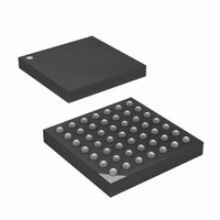
ATXMEGA16A4-CU Atmel, ATXMEGA16A4-CU Datasheet - Page 145

ATXMEGA16A4-CU
Manufacturer Part Number
ATXMEGA16A4-CU
Description
MCU AVR 16+4KB FLASH 49VFBGA
Manufacturer
Atmel
Series
AVR® XMEGAr
Specifications of ATXMEGA16A4-CU
Core Processor
AVR
Core Size
8/16-Bit
Speed
32MHz
Connectivity
I²C, IrDA, SPI, UART/USART
Peripherals
Brown-out Detect/Reset, DMA, POR, PWM, WDT
Number Of I /o
34
Program Memory Size
16KB (8K x 16)
Program Memory Type
FLASH
Eeprom Size
1K x 8
Ram Size
2K x 8
Voltage - Supply (vcc/vdd)
1.6 V ~ 3.6 V
Data Converters
A/D 12x12b, D/A 2x12b
Oscillator Type
Internal
Operating Temperature
-40°C ~ 85°C
Package / Case
49-VFBGA
Processor Series
ATXMEGA16x
Core
AVR8
Data Bus Width
8 bit, 16 bit
Data Ram Size
2 KB
Interface Type
I2C/SPI/USART
Maximum Clock Frequency
32 MHz
Number Of Programmable I/os
34
Number Of Timers
5
Operating Supply Voltage
1.6 V to 3.6 V
Maximum Operating Temperature
+ 85 C
Mounting Style
SMD/SMT
3rd Party Development Tools
EWAVR, EWAVR-BL
Development Tools By Supplier
ATAVRDRAGON, ATAVRISP2, ATAVRONEKIT
Minimum Operating Temperature
- 40 C
On-chip Adc
12-ch x 12-bit
On-chip Dac
2-ch x 12-bit
For Use With
ATAVRONEKIT - KIT AVR/AVR32 DEBUGGER/PROGRMMRATSTK600 - DEV KIT FOR AVR/AVR32770-1007 - ISP 4PORT ATMEL AVR MCU SPI/JTAG770-1004 - ISP 4PORT FOR ATMEL AVR MCU SPI
Lead Free Status / RoHS Status
Lead free / RoHS Compliant
Available stocks
Company
Part Number
Manufacturer
Quantity
Price
- Current page: 145 of 445
- Download datasheet (6Mb)
13.15.4
8077H–AVR–12/09
CLKEVOUT - Clock and Event Out Register
Table 13-6.
• Bit 7:6 - Reserved
These bits are reserved and will always be read as one. For compatibility with future devices,
always write these bits to zero when this register is written.
• Bit 5:4 - EVOUT[1:0] - Event Output Port
These bits decide which port the Event Channel 0 from the Event System should be output to.
Pin 7 on the selected port is always used, and the CLKOUT bits must be set different from
EVOUT. The pin must be configured as an output pin for the Signaling Event to be available on
the pin.
Table 13-7 on page 145
Table 13-7.
• Bits 3:2 - Reserved
These bits are reserved and will always be read as one. For compatibility with future devices,
always write these bits to zero when this register is written.
• Bit 1:0 - CLKOUT[1:0] - Clock Output Port
These bits decide which port the Peripheral Clock should be output to. Pin 7 on the selected port
is always used. The Clock output setting, will override the Event output setting, thus if both are
enabled on the same port pin, the Peripheral Clock will be visible. The pin must be configured as
an output pin for the Clock to be available on the pin.
Table 13-8 on page 146
Bit
+0x04
Read/Write
Initial Value
EVOUT[1:0]
00
01
10
11
VPnMAP[3:0]
1101
1110
1111
R
7
0
-
Virtual Port mapping. (Continued)
Event Channel 0 output configurations
Group Configuration
PORTP
PORTQ
PORTR
6
R
0
-
shows the possible configurations.
shows the possible configurations.
Group Configuration
OFF
PC7
PD7
PE7
R/W
5
0
EVOUT[1:0]
R/W
4
0
Description
Event out disabled
Event Channel 0 output on Port C pin 7
Event Channel 0 output on Port D pin 7
Event Channel 0 output on Port E pin 7
3
R
0
-
Description
PORTP mapped to virtual Port n
PORTQ mapped to virtual Port n
PORTR mapped to virtual Port n
R
2
0
-
R/W
1
0
CLKOUT[1:0]
XMEGA A
R/W
0
0
CLKEVOUT
145
Related parts for ATXMEGA16A4-CU
Image
Part Number
Description
Manufacturer
Datasheet
Request
R

Part Number:
Description:
DEV KIT FOR AVR/AVR32
Manufacturer:
Atmel
Datasheet:

Part Number:
Description:
INTERVAL AND WIPE/WASH WIPER CONTROL IC WITH DELAY
Manufacturer:
ATMEL Corporation
Datasheet:

Part Number:
Description:
Low-Voltage Voice-Switched IC for Hands-Free Operation
Manufacturer:
ATMEL Corporation
Datasheet:

Part Number:
Description:
MONOLITHIC INTEGRATED FEATUREPHONE CIRCUIT
Manufacturer:
ATMEL Corporation
Datasheet:

Part Number:
Description:
AM-FM Receiver IC U4255BM-M
Manufacturer:
ATMEL Corporation
Datasheet:

Part Number:
Description:
Monolithic Integrated Feature Phone Circuit
Manufacturer:
ATMEL Corporation
Datasheet:

Part Number:
Description:
Multistandard Video-IF and Quasi Parallel Sound Processing
Manufacturer:
ATMEL Corporation
Datasheet:

Part Number:
Description:
High-performance EE PLD
Manufacturer:
ATMEL Corporation
Datasheet:

Part Number:
Description:
8-bit Flash Microcontroller
Manufacturer:
ATMEL Corporation
Datasheet:

Part Number:
Description:
2-Wire Serial EEPROM
Manufacturer:
ATMEL Corporation
Datasheet:


