ATXMEGA16A4-CU Atmel, ATXMEGA16A4-CU Datasheet - Page 272
ATXMEGA16A4-CU
Manufacturer Part Number
ATXMEGA16A4-CU
Description
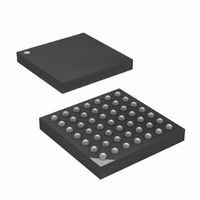
MCU AVR 16+4KB FLASH 49VFBGA
Manufacturer
Atmel
Series
AVR® XMEGAr
Specifications of ATXMEGA16A4-CU
Core Processor
AVR
Core Size
8/16-Bit
Speed
32MHz
Connectivity
I²C, IrDA, SPI, UART/USART
Peripherals
Brown-out Detect/Reset, DMA, POR, PWM, WDT
Number Of I /o
34
Program Memory Size
16KB (8K x 16)
Program Memory Type
FLASH
Eeprom Size
1K x 8
Ram Size
2K x 8
Voltage - Supply (vcc/vdd)
1.6 V ~ 3.6 V
Data Converters
A/D 12x12b, D/A 2x12b
Oscillator Type
Internal
Operating Temperature
-40°C ~ 85°C
Package / Case
49-VFBGA
Processor Series
ATXMEGA16x
Core
AVR8
Data Bus Width
8 bit, 16 bit
Data Ram Size
2 KB
Interface Type
I2C/SPI/USART
Maximum Clock Frequency
32 MHz
Number Of Programmable I/os
34
Number Of Timers
5
Operating Supply Voltage
1.6 V to 3.6 V
Maximum Operating Temperature
+ 85 C
Mounting Style
SMD/SMT
3rd Party Development Tools
EWAVR, EWAVR-BL
Development Tools By Supplier
ATAVRDRAGON, ATAVRISP2, ATAVRONEKIT
Minimum Operating Temperature
- 40 C
On-chip Adc
12-ch x 12-bit
On-chip Dac
2-ch x 12-bit
For Use With
ATAVRONEKIT - KIT AVR/AVR32 DEBUGGER/PROGRMMRATSTK600 - DEV KIT FOR AVR/AVR32770-1007 - ISP 4PORT ATMEL AVR MCU SPI/JTAG770-1004 - ISP 4PORT FOR ATMEL AVR MCU SPI
Lead Free Status / RoHS Status
Lead free / RoHS Compliant
Available stocks
Company
Part Number
Manufacturer
Quantity
Price


24.6.5
24.6.6
24.7
24.7.1
8077H–AVR–12/09
SRAM LPC Configuration
Address Latch Requirements
Timing
Multiplexing Data with Address Byte 0
Figure 24-5. Multiplexed SRAM connection using ALE1 and ALE2
The Address Latch timing and parameter requirements are described in
277.
SRAM or external memory devices may have different timing requirements. To meet these vary-
ing requirements, each Chip Select can be configured with different wait-states. Timing details is
described in
The SRAM Low Pin Count (LPC) configuration enables EBI to be configured for multiplexing
modes where the data and address lines are multiplexed. Compared to SRAM configuration,
this can further reduce the number of pins required for the EBI. The available configurations is
shown in
Timing and Address Latch requirements is as for SRAM configuration.
When the data byte and address byte 0 (AD[7:0]) are multiplexed, they are output from the same
port, and the ALE1 signal from the device controls the address latch.
Figure 24-6. Multiplexed SRAM LPC connection using ALE1
Section 24.7.1 on page 272
”EBI Timing” on page
EBI
EBI
A[23:16]/
A[19:16]
A[15:8]/
AD[7:0]
A[15:8]
D[7:0]
A[7:0]
ALE1
ALE2
ALE1
277.
through
D
G
Q
Section 24.7.2 on page
D
G
D
G
Q
Q
D[7:0]
A[7:0]
A[15:8]
A[23:16]
D[7:0]
A[7:0]
A[15:8]
A[19:16]
273.
SRAM
SRAM
”EBI Timing” on page
XMEGA A
272
Related parts for ATXMEGA16A4-CU
Image
Part Number
Description
Manufacturer
Datasheet
Request
R

Part Number:
Description:
DEV KIT FOR AVR/AVR32
Manufacturer:
Atmel
Datasheet:

Part Number:
Description:
INTERVAL AND WIPE/WASH WIPER CONTROL IC WITH DELAY
Manufacturer:
ATMEL Corporation
Datasheet:
Part Number:
Description:
Low-Voltage Voice-Switched IC for Hands-Free Operation
Manufacturer:
ATMEL Corporation
Datasheet:
Part Number:
Description:
MONOLITHIC INTEGRATED FEATUREPHONE CIRCUIT
Manufacturer:
ATMEL Corporation
Datasheet:
Part Number:
Description:
AM-FM Receiver IC U4255BM-M
Manufacturer:
ATMEL Corporation
Datasheet:
Part Number:
Description:
Monolithic Integrated Feature Phone Circuit
Manufacturer:
ATMEL Corporation
Datasheet:
Part Number:
Description:
Multistandard Video-IF and Quasi Parallel Sound Processing
Manufacturer:
ATMEL Corporation
Datasheet:
Part Number:
Description:
High-performance EE PLD
Manufacturer:
ATMEL Corporation
Datasheet:
Part Number:
Description:
8-bit Flash Microcontroller
Manufacturer:
ATMEL Corporation
Datasheet:
Part Number:
Description:
2-Wire Serial EEPROM
Manufacturer:
ATMEL Corporation
Datasheet: