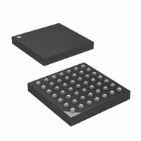
ATXMEGA16A4-CU Atmel, ATXMEGA16A4-CU Datasheet - Page 231

ATXMEGA16A4-CU
Manufacturer Part Number
ATXMEGA16A4-CU
Description
MCU AVR 16+4KB FLASH 49VFBGA
Manufacturer
Atmel
Series
AVR® XMEGAr
Specifications of ATXMEGA16A4-CU
Core Processor
AVR
Core Size
8/16-Bit
Speed
32MHz
Connectivity
I²C, IrDA, SPI, UART/USART
Peripherals
Brown-out Detect/Reset, DMA, POR, PWM, WDT
Number Of I /o
34
Program Memory Size
16KB (8K x 16)
Program Memory Type
FLASH
Eeprom Size
1K x 8
Ram Size
2K x 8
Voltage - Supply (vcc/vdd)
1.6 V ~ 3.6 V
Data Converters
A/D 12x12b, D/A 2x12b
Oscillator Type
Internal
Operating Temperature
-40°C ~ 85°C
Package / Case
49-VFBGA
Processor Series
ATXMEGA16x
Core
AVR8
Data Bus Width
8 bit, 16 bit
Data Ram Size
2 KB
Interface Type
I2C/SPI/USART
Maximum Clock Frequency
32 MHz
Number Of Programmable I/os
34
Number Of Timers
5
Operating Supply Voltage
1.6 V to 3.6 V
Maximum Operating Temperature
+ 85 C
Mounting Style
SMD/SMT
3rd Party Development Tools
EWAVR, EWAVR-BL
Development Tools By Supplier
ATAVRDRAGON, ATAVRISP2, ATAVRONEKIT
Minimum Operating Temperature
- 40 C
On-chip Adc
12-ch x 12-bit
On-chip Dac
2-ch x 12-bit
For Use With
ATAVRONEKIT - KIT AVR/AVR32 DEBUGGER/PROGRMMRATSTK600 - DEV KIT FOR AVR/AVR32770-1007 - ISP 4PORT ATMEL AVR MCU SPI/JTAG770-1004 - ISP 4PORT FOR ATMEL AVR MCU SPI
Lead Free Status / RoHS Status
Lead free / RoHS Compliant
Available stocks
Company
Part Number
Manufacturer
Quantity
Price
- Current page: 231 of 445
- Download datasheet (6Mb)
20.5
8077H–AVR–12/09
Data Modes
As the SS pin is used to signal start and end of transfer, it is also useful for doing packet/byte
synchronization, keeping the Slave bit counter synchronous with the Master clock generator.
There are four combinations of SCK phase and polarity with respect to serial data. The SPI data
transfer formats are shown in
edges of the SCK signal, ensuring sufficient time for data signals to stabilize.
Table 20-2.
Leading edge is the first clock edge in a clock cycle. Trailing edge is the last clock edge in a
clock cycle.
Figure 20-2. SPI Transfer modes
Mode
Mode 0
Mode 2
SAMPLE I
MOSI/MISO
CHANGE 0
MOSI PIN
CHANGE 0
MISO PIN
Mode 1
Mode 3
SAMPLE I
MOSI/MISO
CHANGE 0
MOSI PIN
CHANGE 0
MISO PIN
SS
SS
0
1
2
3
MSB first (DORD = 0)
LSB first (DORD = 1)
MSB first (DORD = 0)
LSB first (DORD = 1)
SPI Modes
MSB
LSB
Figure
MSB
LSB
Bit 6
Bit 1
Rising, Sample
Leading Edge
Falling,Sample
20-2. Data bits are shifted out and latched in on opposite
Falling, Setup
Rising, Setup
Bit 6
Bit 1
Bit 5
Bit 2
Bit 5
Bit 2
Bit 4
Bit 3
Bit 4
Bit 3
Bit 3
Bit 4
Bit 3
Bit 4
Bit 2
Bit 5
Bit 2
Bit 5
Bit 1
Bit 6
Falling, Sample
Rising, Sample
Trailing Edge
Falling, Setup
Rising, Setup
Bit 1
Bit 6
LSB
MSB
XMEGA A
LSB
MSB
231
Related parts for ATXMEGA16A4-CU
Image
Part Number
Description
Manufacturer
Datasheet
Request
R

Part Number:
Description:
DEV KIT FOR AVR/AVR32
Manufacturer:
Atmel
Datasheet:

Part Number:
Description:
INTERVAL AND WIPE/WASH WIPER CONTROL IC WITH DELAY
Manufacturer:
ATMEL Corporation
Datasheet:

Part Number:
Description:
Low-Voltage Voice-Switched IC for Hands-Free Operation
Manufacturer:
ATMEL Corporation
Datasheet:

Part Number:
Description:
MONOLITHIC INTEGRATED FEATUREPHONE CIRCUIT
Manufacturer:
ATMEL Corporation
Datasheet:

Part Number:
Description:
AM-FM Receiver IC U4255BM-M
Manufacturer:
ATMEL Corporation
Datasheet:

Part Number:
Description:
Monolithic Integrated Feature Phone Circuit
Manufacturer:
ATMEL Corporation
Datasheet:

Part Number:
Description:
Multistandard Video-IF and Quasi Parallel Sound Processing
Manufacturer:
ATMEL Corporation
Datasheet:

Part Number:
Description:
High-performance EE PLD
Manufacturer:
ATMEL Corporation
Datasheet:

Part Number:
Description:
8-bit Flash Microcontroller
Manufacturer:
ATMEL Corporation
Datasheet:

Part Number:
Description:
2-Wire Serial EEPROM
Manufacturer:
ATMEL Corporation
Datasheet:


