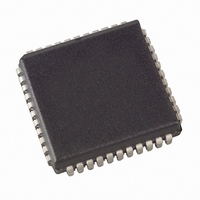
AT89C51RE2-SLRUM Atmel, AT89C51RE2-SLRUM Datasheet - Page 15

AT89C51RE2-SLRUM
Manufacturer Part Number
AT89C51RE2-SLRUM
Description
MCU 8051 128K FLASH 44-PLCC
Manufacturer
Atmel
Series
89Cr
Datasheet
1.AT89C51RE2-SLSUM.pdf
(187 pages)
Specifications of AT89C51RE2-SLRUM
Core Processor
8051
Core Size
8-Bit
Speed
60MHz
Connectivity
I²C, SPI, UART/USART
Peripherals
POR, PWM, WDT
Number Of I /o
34
Program Memory Size
128KB (128K x 8)
Program Memory Type
FLASH
Ram Size
8K x 8
Voltage - Supply (vcc/vdd)
2.7 V ~ 5.5 V
Oscillator Type
External
Operating Temperature
-40°C ~ 85°C
Package / Case
44-PLCC
Processor Series
AT89x
Core
8051
Data Bus Width
8 bit
Data Ram Size
8 KB
Interface Type
UART, SPI
Maximum Clock Frequency
60 MHz
Number Of Programmable I/os
34
Number Of Timers
3
Operating Supply Voltage
2.7 V to 5.5 V
Mounting Style
SMD/SMT
3rd Party Development Tools
PK51, CA51, A51, ULINK2
Development Tools By Supplier
AT89OCD-01
For Use With
AT89STK-11 - KIT STARTER FOR AT89C51RX2
Lead Free Status / RoHS Status
Lead free / RoHS Compliant
Eeprom Size
-
Data Converters
-
Lead Free Status / Rohs Status
Details
Available stocks
Company
Part Number
Manufacturer
Quantity
Price
Company:
Part Number:
AT89C51RE2-SLRUM
Manufacturer:
Atmel
Quantity:
759
7663E–8051–10/08
Table 15. CKCON0 Register
CKCON0 - Clock Control Register (8Fh)
Reset Value = X000 000’HSB. X2’b (See “Fuse Configuration Byte: FCB”)
Not bit addressable
Number
TWIX2
Bit
7
7
6
5
4
3
2
1
0
Mnemonic
WDX2
PCAX2
SIX2_0
TWIX2
WDX2
T2X2
T1X2
T0X2
Bit
X2
6
Description
2-wire cloTBck
(This control bit is validated when the CPU clock X2 is set; when X2 is low, this bit has no
effect)
Cleared to select 6 clock periods per peripheral clock cycle.
Set to select 12 clock periods per peripheral clock cycle.
Watchdog Clock
(This control bit is validated when the CPU clock X2 is set; when X2 is low, this bit has no
effect).
Cleared to select 6 clock periods per peripheral clock cycle.
Set to select 12 clock periods per peripheral clock cycle.
Programmable Counter Array Clock
(This control bit is validated when the CPU clock X2 is set; when X2 is low, this bit has no
effect).
Cleared to select 6 clock periods per peripheral clock cycle. Set to select 12 clock
periods per peripheral clock cycle.
Enhanced UART0 Clock (Mode 0 and 2)
(This control bit is validated when the CPU clock X2 is set; when X2 is low, this bit has no
effect).
Cleared to select 6 clock periods per peripheral clock cycle. Set to select 12 clock
periods per peripheral clock cycle.
Timer2 Clock
(This control bit is validated when the CPU clock X2 is set; when X2 is low, this bit has no
effect).
Cleared to select 6 clock periods per peripheral clock cycle.
Set to select 12 clock periods per peripheral clock cycle.
Timer1 Clock
(This control bit is validated when the CPU clock X2 is set; when X2 is low, this bit has no
effect).
Cleared to select 6 clock periods per peripheral clock cycle. Set to select 12 clock
periods per peripheral clock cycle.
Timer0 Clock
(This control bit is validated when the CPU clock X2 is set; when X2 is low, this bit has no
effect).
Cleared to select 6 clock periods per peripheral clock cycle. Set to select 12 clock
periods per peripheral clock cycle.
CPU Clock
Cleared to select 12 clock periods per machine cycle (STD mode) for CPU and all the
peripherals. Set to select 6clock periods per machine cycle (X2 mode) and to enable the
individual peripherals’X2’ bits. Programmed by hardware after Power-up regarding
Hardware Security Byte (HSB), Default setting, X2 is cleared.
PCAX2
5
SIX2_0
4
T2X2
3
T1X2
2
AT89C51RE2
T0X2
1
X2
0
15


