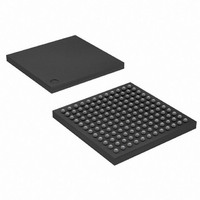
ATSAM3U4EA-CU Atmel, ATSAM3U4EA-CU Datasheet - Page 1079

ATSAM3U4EA-CU
Manufacturer Part Number
ATSAM3U4EA-CU
Description
IC MCU 32BIT 256KB FLSH 144LFBGA
Manufacturer
Atmel
Series
SAM3Ur
Specifications of ATSAM3U4EA-CU
Core Processor
ARM® Cortex-M3™
Core Size
32-Bit
Speed
96MHz
Connectivity
EBI/EMI, I²C, MMC, SPI, SSC, UART/USART, USB
Peripherals
Brown-out Detect/Reset, DMA, I²S, POR, PWM, WDT
Number Of I /o
96
Program Memory Size
256KB (256K x 8)
Program Memory Type
FLASH
Ram Size
52K x 8
Voltage - Supply (vcc/vdd)
1.65 V ~ 1.95 V
Data Converters
A/D 8x10b, 8x12b
Oscillator Type
Internal
Operating Temperature
-40°C ~ 85°C
Package / Case
144-LFBGA
Processor Series
ATSAM3x
Core
ARM Cortex M3
Data Bus Width
32 bit
Data Ram Size
52 KB
Interface Type
4xUSART, 2xTWI, 5xSPI, Bus
Maximum Clock Frequency
96 MHz
Number Of Programmable I/os
96
Number Of Timers
8
Operating Supply Voltage
1.62 V to 3.6 V
Maximum Operating Temperature
+ 85 C
Mounting Style
SMD/SMT
3rd Party Development Tools
JTRACE-CM3, AT91SAM3U-EK, MDK-ARM, RL-ARM, ULINK2
Development Tools By Supplier
ATSAM3U-EK
Minimum Operating Temperature
- 40 C
Lead Free Status / RoHS Status
Lead free / RoHS Compliant
Eeprom Size
-
Lead Free Status / Rohs Status
Details
Available stocks
Company
Part Number
Manufacturer
Quantity
Price
- Current page: 1079 of 1171
- Download datasheet (25Mb)
42. Analog-to-Digital Converter (ADC)
42.1
42.2
Figure 42-1. Analog-to-Digital Converter Block Diagram
42.3
Table 42-1.
6430D–ATARM–25-Mar-11
Pin Name
AD0 - AD7
ADTRG
Description
Block Diagram
Signal Description
Analog Inputs
with I/O lines
Multiplexed
ADC Pin Description
VDDANA
ADVREF
ADTRG
The ADC is based on a Successive Approximation Register (SAR) 10-bit Analog-to-Digital Con-
verter (ADC). It also integrates an 8-to-1 analog multiplexer, making possible the analog-to-
digital conversions of 8 analog lines. The conversions extend from 0V to ADVREF. The ADC
supports an 8-bit or 10-bit resolution mode, and conversion results are reported in a common
register for all channels, as well as in a channel-dedicated register. Software trigger, external
trigger on rising edge of the ADTRG pin or internal triggers from Timer Counter output(s) or
PWM Event lines are configurable.
The ADC also integrates a Sleep Mode and a conversion sequencer and connects with a PDC
channel. These features reduce both power consumption and processor intervention.
Finally, the user can configure ADC timings, such as Startup Time and Sample & Hold Time.
GND
AD0
AD1
ADn
PIO
Description
Analog input channels
External trigger
Selection
Channels
Trigger
Counter
Timer
Analog-to-Digital
Approximation
ADC cell
Successive
Converter
Register
ADC Controller
Interface
PMC
Control
Logic
User
MCK
ADC Interrupt
PDC
NVIC
SAM3U Series
System Bus
Peripheral Bridge
APB
1079
Related parts for ATSAM3U4EA-CU
Image
Part Number
Description
Manufacturer
Datasheet
Request
R

Part Number:
Description:
KIT EVAL FOR AT91SAM3U CORTEX
Manufacturer:
Atmel
Datasheet:

Part Number:
Description:
AT91 ARM Thumb-based Microcontrollers
Manufacturer:
ATMEL [ATMEL Corporation]
Datasheet:

Part Number:
Description:
DEV KIT FOR AVR/AVR32
Manufacturer:
Atmel
Datasheet:

Part Number:
Description:
INTERVAL AND WIPE/WASH WIPER CONTROL IC WITH DELAY
Manufacturer:
ATMEL Corporation
Datasheet:

Part Number:
Description:
Low-Voltage Voice-Switched IC for Hands-Free Operation
Manufacturer:
ATMEL Corporation
Datasheet:

Part Number:
Description:
MONOLITHIC INTEGRATED FEATUREPHONE CIRCUIT
Manufacturer:
ATMEL Corporation
Datasheet:

Part Number:
Description:
AM-FM Receiver IC U4255BM-M
Manufacturer:
ATMEL Corporation
Datasheet:

Part Number:
Description:
Monolithic Integrated Feature Phone Circuit
Manufacturer:
ATMEL Corporation
Datasheet:

Part Number:
Description:
Multistandard Video-IF and Quasi Parallel Sound Processing
Manufacturer:
ATMEL Corporation
Datasheet:

Part Number:
Description:
High-performance EE PLD
Manufacturer:
ATMEL Corporation
Datasheet:

Part Number:
Description:
8-bit Flash Microcontroller
Manufacturer:
ATMEL Corporation
Datasheet:

Part Number:
Description:
2-Wire Serial EEPROM
Manufacturer:
ATMEL Corporation
Datasheet:


