AT91SAM9XE512-CU Atmel, AT91SAM9XE512-CU Datasheet - Page 150
AT91SAM9XE512-CU
Manufacturer Part Number
AT91SAM9XE512-CU
Description
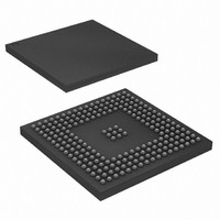
MCU ARM9 512K FLASH 217-BGA
Manufacturer
Atmel
Series
AT91SAMr
Datasheet
1.AT91SAM9XE128-QU.pdf
(860 pages)
Specifications of AT91SAM9XE512-CU
Core Processor
ARM9
Core Size
16/32-Bit
Speed
180MHz
Connectivity
EBI/EMI, Ethernet, I²C, MMC, SPI, SSC, UART/USART, USB
Peripherals
Brown-out Detect/Reset, POR, PWM, WDT
Number Of I /o
96
Program Memory Size
512KB (512K x 8)
Program Memory Type
FLASH
Ram Size
56K x 8
Voltage - Supply (vcc/vdd)
1.65 V ~ 1.95 V
Data Converters
A/D 4x10b
Oscillator Type
Internal
Operating Temperature
-40°C ~ 85°C
Package / Case
217-LFBGA
Package
217LFBGA
Device Core
ARM926EJ-S
Family Name
91S
Maximum Speed
180 MHz
Operating Supply Voltage
1.8|2.5|3.3 V
Data Bus Width
32 Bit
Number Of Programmable I/os
96
Interface Type
EBI/Ethernet/SPI/TWI/USART/USB
On-chip Adc
4-chx10-bit
Number Of Timers
6
Processor Series
AT91SAMx
Core
ARM926EJ-S
Data Ram Size
32 KB
Maximum Clock Frequency
180 MHz
Maximum Operating Temperature
+ 85 C
Mounting Style
SMD/SMT
3rd Party Development Tools
JTRACE-ARM-2M, KSK-AT91SAM9XE-PL, MDK-ARM, RL-ARM, ULINK2
Development Tools By Supplier
AT91SAM-ICE, AT91-ISP, AT91SAM9XE-EK
Minimum Operating Temperature
- 40 C
For Use With
AT91SAM9XE-EK - KIT EVAL FOR AT91SAM9XEAT91SAM-ICE - EMULATOR FOR AT91 ARM7/ARM9
Lead Free Status / RoHS Status
Lead free / RoHS Compliant
Eeprom Size
-
Lead Free Status / Rohs Status
Details
Available stocks
Company
Part Number
Manufacturer
Quantity
Price
Company:

Part Number:
AT91SAM9XE512-CU
Manufacturer:
NEC
Quantity:
201
Part Number:
AT91SAM9XE512-CU
Manufacturer:
ATMEL/爱特梅尔
Quantity:
20 000


Table 20-2.
20.3.3.2
150
Symbol
FL_ID
FL_SIZE
FL_PAGE_SIZE
FL_NB_PLANE
FL_PLANE[0]
...
FL_PLANE[FL_NB_PLANE-1]
FL_NB_LOCK
FL_LOCK[0]
...
AT91SAM9XE128/256/512 Preliminary
Write Commands
Flash Descriptor Definition
ations to the EEFC_FRR register are done after the last word of the descriptor has been
returned, then the EEFC_FRR register value is 0 until the next valid command.
Several commands can be used to program the Flash.
Flash technology requires that an erase is done before programming. The full memory plane can
be erased at the same time, or several pages can be erased at the same time (refer to
Commands” on page
using EWP or EWPL commands.
After programming, the page (the whole lock region) can be locked to prevent miscellaneous
write or erase sequences. The lock bit can be automatically set after page programming using
WPL or EWPL commands.
Data to be written are stored in an internal latch buffer. The size of the latch buffer corresponds
to the page size. The latch buffer wraps around within the internal memory area address space
and is repeated as many times as the number of pages within this address space.
Note:
Write operations are performed in a number of wait states equal to the number of wait states for
read operations.
Data are written to the latch buffer before the programming command is written to the Flash
Command Register EEFC_FCR. The sequence is as follows:
Two errors can be detected in the EEFC_FSR register after a programming sequence:
• Write the full page, at any page address, within the internal memory area address space.
• Programming starts as soon as the page number and the programming command are written
• When programming is completed, the bit FRDY in the Flash Programming Status Register
to the Flash Command Register. The FRDY bit in the Flash Programming Status Register
(EEFC_FSR) is automatically cleared.
(EEFC_FSR) rises. If an interrupt has been enabled by setting the bit FRDY in EEFC_FMR,
the interrupt line of the System Controller is activated.
Writing of 8-bit and 16-bit data is not allowed and may lead to unpredictable data corruption.
Word Index
0
1
2
3
4
4 + FL_NB_PLANE - 1
4 + FL_NB_PLANE
4 + FL_NB_PLANE + 1
151). Also, a page erase can be automatically done before a page write
Number of bytes in the first lock region.
Description
Flash Interface Description
Flash size in bytes
Page size in bytes
Number of planes.
Number of bytes in the first plane.
Number of bytes in the last plane.
Number of lock bits. A bit is associated
with a lock region. A lock bit is used to
prevent write or erase operations in the
lock region.
6254C–ATARM–22-Jan-10
“Erase
Related parts for AT91SAM9XE512-CU
Image
Part Number
Description
Manufacturer
Datasheet
Request
R

Part Number:
Description:
KIT EVAL FOR AT91SAM9XE
Manufacturer:
Atmel
Datasheet:

Part Number:
Description:
MCU ARM9 64K SRAM 144-LFBGA
Manufacturer:
Atmel
Datasheet:

Part Number:
Description:
IC ARM7 MCU FLASH 256K 100LQFP
Manufacturer:
Atmel
Datasheet:

Part Number:
Description:
IC ARM9 MPU 217-LFBGA
Manufacturer:
Atmel
Datasheet:
Part Number:
Description:
MCU ARM9 ULTRA LOW PWR 217-LFBGA
Manufacturer:
Atmel
Datasheet:

Part Number:
Description:
MCU ARM9 324-TFBGA
Manufacturer:
Atmel
Datasheet:
Part Number:
Description:
IC MCU ARM9 SAMPLING 217CBGA
Manufacturer:
Atmel
Datasheet:
Part Number:
Description:
IC ARM9 MCU 217-LFBGA
Manufacturer:
Atmel
Datasheet:

Part Number:
Description:
IC ARM9 MCU 208-PQFP
Manufacturer:
Atmel
Datasheet:
Part Number:
Description:
MCU ARM 512K HS FLASH 100-LQFP
Manufacturer:
Atmel
Datasheet:

Part Number:
Description:
MCU ARM 512K HS FLASH 100-TFBGA
Manufacturer:
Atmel
Datasheet:
Part Number:
Description:
IC ARM9 MCU 200 MHZ 324-TFBGA
Manufacturer:
Atmel
Datasheet:

Part Number:
Description:
IC ARM MCU 16BIT 128K 256BGA
Manufacturer:
Atmel
Datasheet:

Part Number:
Description:
IC ARM7 MCU 32BIT 128K 64LQFP
Manufacturer:
Atmel
Datasheet:

Part Number:
Description:
IC ARM7 MCU FLASH 256K 128-LQFP
Manufacturer:
Atmel
Datasheet: