AT91SAM9XE512-CU Atmel, AT91SAM9XE512-CU Datasheet - Page 830
AT91SAM9XE512-CU
Manufacturer Part Number
AT91SAM9XE512-CU
Description
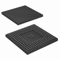
MCU ARM9 512K FLASH 217-BGA
Manufacturer
Atmel
Series
AT91SAMr
Datasheet
1.AT91SAM9XE128-QU.pdf
(860 pages)
Specifications of AT91SAM9XE512-CU
Core Processor
ARM9
Core Size
16/32-Bit
Speed
180MHz
Connectivity
EBI/EMI, Ethernet, I²C, MMC, SPI, SSC, UART/USART, USB
Peripherals
Brown-out Detect/Reset, POR, PWM, WDT
Number Of I /o
96
Program Memory Size
512KB (512K x 8)
Program Memory Type
FLASH
Ram Size
56K x 8
Voltage - Supply (vcc/vdd)
1.65 V ~ 1.95 V
Data Converters
A/D 4x10b
Oscillator Type
Internal
Operating Temperature
-40°C ~ 85°C
Package / Case
217-LFBGA
Package
217LFBGA
Device Core
ARM926EJ-S
Family Name
91S
Maximum Speed
180 MHz
Operating Supply Voltage
1.8|2.5|3.3 V
Data Bus Width
32 Bit
Number Of Programmable I/os
96
Interface Type
EBI/Ethernet/SPI/TWI/USART/USB
On-chip Adc
4-chx10-bit
Number Of Timers
6
Processor Series
AT91SAMx
Core
ARM926EJ-S
Data Ram Size
32 KB
Maximum Clock Frequency
180 MHz
Maximum Operating Temperature
+ 85 C
Mounting Style
SMD/SMT
3rd Party Development Tools
JTRACE-ARM-2M, KSK-AT91SAM9XE-PL, MDK-ARM, RL-ARM, ULINK2
Development Tools By Supplier
AT91SAM-ICE, AT91-ISP, AT91SAM9XE-EK
Minimum Operating Temperature
- 40 C
For Use With
AT91SAM9XE-EK - KIT EVAL FOR AT91SAM9XEAT91SAM-ICE - EMULATOR FOR AT91 ARM7/ARM9
Lead Free Status / RoHS Status
Lead free / RoHS Compliant
Eeprom Size
-
Lead Free Status / Rohs Status
Details
Available stocks
Company
Part Number
Manufacturer
Quantity
Price
Company:

Part Number:
AT91SAM9XE512-CU
Manufacturer:
NEC
Quantity:
201
Part Number:
AT91SAM9XE512-CU
Manufacturer:
ATMEL/爱特梅尔
Quantity:
20 000


43.15.4
Table 43-46. MCI Timings
830
Symbol
MCI
MCI
MCI
MCI
MCI
1
2
3
4
5
AT91SAM9XE128/256/512 Preliminary
MCI
Parameter
CLK frequency at Data transfer Mode
CLK frequency at Identification Mode
CLK Low time
CLK High time
CLK Rise time
CLK Fall time
CLK Low time
CLK High time
CLK Rise time
CLK Fall time
Input hold time
Input setup time
Output change after CLK rising
Output valid before CLK rising
The PDC interface block controls all data routing between the external data bus, internal
MMC/SD module data bus, and internal system FIFO access through a dedicated state machine
that monitors the status of FIFO content (empty or full), FIFO address, and byte/block counters
for the MMC/SD module (inner system) and the application (user programming).
These timings are given for a 25 pF load, corresponding to 1 MMC/SD Card.
Figure 43-20. MCI Timing Diagram
CMD_DAT Output
CMD_DAT Input
Bus Clock
5a
Valid Data
C = 100 pf
C = 250 pf
C = 100 pf
C = 100 pf
C = 100 pf
C = 100 pf
C = 250 pf
C = 250 pf
C = 250 pf
C = 250 pf
C = 25 pf
CLoad
3a
4a
5
3b
6a
Valid Data
Min
10
10
50
50
3
3
5
1
7
2
Valid Data
Valid Data
Max
400
25
20
20
10
10
50
50
6b
5b
4b
6254C–ATARM–22-Jan-10
Units
MHz
MHz
MHz
kHz
ns
ns
ns
ns
ns
ns
ns
ns
ns
ns
ns
ns
Related parts for AT91SAM9XE512-CU
Image
Part Number
Description
Manufacturer
Datasheet
Request
R

Part Number:
Description:
KIT EVAL FOR AT91SAM9XE
Manufacturer:
Atmel
Datasheet:

Part Number:
Description:
MCU ARM9 64K SRAM 144-LFBGA
Manufacturer:
Atmel
Datasheet:

Part Number:
Description:
IC ARM7 MCU FLASH 256K 100LQFP
Manufacturer:
Atmel
Datasheet:

Part Number:
Description:
IC ARM9 MPU 217-LFBGA
Manufacturer:
Atmel
Datasheet:
Part Number:
Description:
MCU ARM9 ULTRA LOW PWR 217-LFBGA
Manufacturer:
Atmel
Datasheet:

Part Number:
Description:
MCU ARM9 324-TFBGA
Manufacturer:
Atmel
Datasheet:
Part Number:
Description:
IC MCU ARM9 SAMPLING 217CBGA
Manufacturer:
Atmel
Datasheet:
Part Number:
Description:
IC ARM9 MCU 217-LFBGA
Manufacturer:
Atmel
Datasheet:

Part Number:
Description:
IC ARM9 MCU 208-PQFP
Manufacturer:
Atmel
Datasheet:
Part Number:
Description:
MCU ARM 512K HS FLASH 100-LQFP
Manufacturer:
Atmel
Datasheet:

Part Number:
Description:
MCU ARM 512K HS FLASH 100-TFBGA
Manufacturer:
Atmel
Datasheet:
Part Number:
Description:
IC ARM9 MCU 200 MHZ 324-TFBGA
Manufacturer:
Atmel
Datasheet:

Part Number:
Description:
IC ARM MCU 16BIT 128K 256BGA
Manufacturer:
Atmel
Datasheet:

Part Number:
Description:
IC ARM7 MCU 32BIT 128K 64LQFP
Manufacturer:
Atmel
Datasheet:

Part Number:
Description:
IC ARM7 MCU FLASH 256K 128-LQFP
Manufacturer:
Atmel
Datasheet: