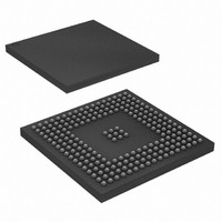
AT91SAM9XE512-CU Atmel, AT91SAM9XE512-CU Datasheet - Page 323

AT91SAM9XE512-CU
Manufacturer Part Number
AT91SAM9XE512-CU
Description
MCU ARM9 512K FLASH 217-BGA
Manufacturer
Atmel
Series
AT91SAMr
Datasheet
1.AT91SAM9XE128-QU.pdf
(860 pages)
Specifications of AT91SAM9XE512-CU
Core Processor
ARM9
Core Size
16/32-Bit
Speed
180MHz
Connectivity
EBI/EMI, Ethernet, I²C, MMC, SPI, SSC, UART/USART, USB
Peripherals
Brown-out Detect/Reset, POR, PWM, WDT
Number Of I /o
96
Program Memory Size
512KB (512K x 8)
Program Memory Type
FLASH
Ram Size
56K x 8
Voltage - Supply (vcc/vdd)
1.65 V ~ 1.95 V
Data Converters
A/D 4x10b
Oscillator Type
Internal
Operating Temperature
-40°C ~ 85°C
Package / Case
217-LFBGA
Package
217LFBGA
Device Core
ARM926EJ-S
Family Name
91S
Maximum Speed
180 MHz
Operating Supply Voltage
1.8|2.5|3.3 V
Data Bus Width
32 Bit
Number Of Programmable I/os
96
Interface Type
EBI/Ethernet/SPI/TWI/USART/USB
On-chip Adc
4-chx10-bit
Number Of Timers
6
Processor Series
AT91SAMx
Core
ARM926EJ-S
Data Ram Size
32 KB
Maximum Clock Frequency
180 MHz
Maximum Operating Temperature
+ 85 C
Mounting Style
SMD/SMT
3rd Party Development Tools
JTRACE-ARM-2M, KSK-AT91SAM9XE-PL, MDK-ARM, RL-ARM, ULINK2
Development Tools By Supplier
AT91SAM-ICE, AT91-ISP, AT91SAM9XE-EK
Minimum Operating Temperature
- 40 C
For Use With
AT91SAM9XE-EK - KIT EVAL FOR AT91SAM9XEAT91SAM-ICE - EMULATOR FOR AT91 ARM7/ARM9
Lead Free Status / RoHS Status
Lead free / RoHS Compliant
Eeprom Size
-
Lead Free Status / Rohs Status
Details
Available stocks
Company
Part Number
Manufacturer
Quantity
Price
Company:
Part Number:
AT91SAM9XE512-CU
Manufacturer:
NEC
Quantity:
201
Part Number:
AT91SAM9XE512-CU
Manufacturer:
ATMEL/爱特梅尔
Quantity:
20 000
- Current page: 323 of 860
- Download datasheet (13Mb)
28.7
6254C–ATARM–22-Jan-10
Programming Sequence
Moreover, like the PCK, a status bitin PMC_SR indicates that the Programmable Clock is actu-
ally what has been programmed in the Programmable Clock registers.
As the Programmable Clock Controller does not manage with glitch prevention when switching
clocks, it is strongly recommended to disable the Programmable Clock before any configuration
change and to re-enable it after the change is actually performed.
1. Enabling the Main Oscillator:
2. Checking the Main Oscillator Frequency (Optional):
3. Setting PLL A and divider A:
The main oscillator is enabled by setting the MOSCEN field in the CKGR_MOR register. In
some cases it may be advantageous to define a start-up time. This can be achieved by writ-
ing a value in the OSCOUNT field in the CKGR_MOR register.
Once this register has been correctly configured, the user must wait for MOSCS field in the
PMC_SR register to be set. This can be done either by polling the status register or by wait-
ing the interrupt line to be raised if the associated interrupt to MOSCS has been enabled in
the PMC_IER register.
Code Example:
Start Up Time = 8 * OSCOUNT / SLCK = 56 Slow Clock Cycles.
So, the main oscillator will be enabled (MOSCS bit set) after 56 Slow Clock Cycles.
In some situations the user may need an accurate measure of the main oscillator frequency.
This measure can be accomplished via the CKGR_MCFR register.
Once the MAINRDY field is set in CKGR_MCFR register, the user may read the MAINF field
in CKGR_MCFR register. This provides the number of main clock cycles within sixteen slow
clock cycles.
All parameters necessary to configure PLL A and divider A are located in the CKGR_PLLAR
register. ICPPLLA in PMC_PLLICPR register must be set to 1 before configuring the
CKGR_PLLAR register.
It is important to note that Bit 29 must always be set to 1 when programming the
CKGR_PLLAR register.
The DIVA field is used to control the divider A itself. The user can program a value between
0 and 255. Divider A output is divider A input divided by DIVA. By default, DIVA parameter is
set to 0 which means that divider A is turned off.
The OUTA field is used to select the PLL A output frequency range.
The MULA field is the PLL A multiplier factor. This parameter can be programmed between
0 and 2047. If MULA is set to 0, PLL A will be turned off. Otherwise PLL A output frequency
is PLL A input frequency multiplied by (MULA + 1).
The PLLACOUNT field specifies the number of slow clock cycles before LOCKA bit is set in
the PMC_SR register after CKGR_PLLAR register has been written.
Once CKGR_PLLAR register has been written, the user is obliged to wait for the LOCKA bit
to be set in the PMC_SR register. This can be done either by polling the status register or by
write_register(CKGR_MOR,0x00000701)
AT91SAM9XE128/256/512 Preliminary
323
Related parts for AT91SAM9XE512-CU
Image
Part Number
Description
Manufacturer
Datasheet
Request
R

Part Number:
Description:
KIT EVAL FOR AT91SAM9XE
Manufacturer:
Atmel
Datasheet:

Part Number:
Description:
MCU ARM9 64K SRAM 144-LFBGA
Manufacturer:
Atmel
Datasheet:

Part Number:
Description:
IC ARM7 MCU FLASH 256K 100LQFP
Manufacturer:
Atmel
Datasheet:

Part Number:
Description:
IC ARM9 MPU 217-LFBGA
Manufacturer:
Atmel
Datasheet:

Part Number:
Description:
MCU ARM9 ULTRA LOW PWR 217-LFBGA
Manufacturer:
Atmel
Datasheet:

Part Number:
Description:
MCU ARM9 324-TFBGA
Manufacturer:
Atmel
Datasheet:

Part Number:
Description:
IC MCU ARM9 SAMPLING 217CBGA
Manufacturer:
Atmel
Datasheet:

Part Number:
Description:
IC ARM9 MCU 217-LFBGA
Manufacturer:
Atmel
Datasheet:

Part Number:
Description:
IC ARM9 MCU 208-PQFP
Manufacturer:
Atmel
Datasheet:

Part Number:
Description:
MCU ARM 512K HS FLASH 100-LQFP
Manufacturer:
Atmel
Datasheet:

Part Number:
Description:
MCU ARM 512K HS FLASH 100-TFBGA
Manufacturer:
Atmel
Datasheet:

Part Number:
Description:
IC ARM9 MCU 200 MHZ 324-TFBGA
Manufacturer:
Atmel
Datasheet:

Part Number:
Description:
IC ARM MCU 16BIT 128K 256BGA
Manufacturer:
Atmel
Datasheet:

Part Number:
Description:
IC ARM7 MCU 32BIT 128K 64LQFP
Manufacturer:
Atmel
Datasheet:

Part Number:
Description:
IC ARM7 MCU FLASH 256K 128-LQFP
Manufacturer:
Atmel
Datasheet:


