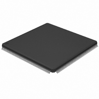
LPC2939FBD208,551 NXP Semiconductors, LPC2939FBD208,551 Datasheet - Page 25

LPC2939FBD208,551
Manufacturer Part Number
LPC2939FBD208,551
Description
IC ARM9 MCU FLASH 768KB 208-LQFP
Manufacturer
NXP Semiconductors
Series
LPC2900r
Datasheet
1.LPC2939FBD208551.pdf
(99 pages)
Specifications of LPC2939FBD208,551
Core Processor
ARM9
Core Size
32-Bit
Speed
125MHz
Connectivity
CAN, EBI/EMI, I²C, LIN, SPI, UART/USART, USB, USB OTG
Peripherals
DMA, POR, PWM, WDT
Number Of I /o
152
Program Memory Size
768KB (768K x 8)
Program Memory Type
FLASH
Eeprom Size
16K x 8
Ram Size
56K x 8
Voltage - Supply (vcc/vdd)
1.71 V ~ 3.6 V
Data Converters
A/D 24x10b
Oscillator Type
Internal
Operating Temperature
-40°C ~ 85°C
Package / Case
208-LQFP
Processor Series
LPC29
Core
ARM968E-S
3rd Party Development Tools
MDK-ARM, RL-ARM, ULINK2
Development Tools By Supplier
OM11027
Package
208LQFP
Device Core
ARM968E-S
Family Name
LPC2900
Operating Supply Voltage
1.8|3.3 V
Data Bus Width
16|32 Bit
Number Of Programmable I/os
160
Interface Type
CAN/I2C/LIN/QSPI/UART/USB
On-chip Adc
24-chx10-bit
Number Of Timers
6
For Use With
568-4787 - BOARD EVAL LPC2939
Lead Free Status / RoHS Status
Lead free / RoHS Compliant
Other names
935287113551
Available stocks
Company
Part Number
Manufacturer
Quantity
Price
Company:
Part Number:
LPC2939FBD208,551
Manufacturer:
NXP Semiconductors
Quantity:
10 000
NXP Semiconductors
LPC2939_3
Product data sheet
6.8.5 Clock description
6.8.6 EEPROM
6.9.1 Description
6.9 External Static Memory Controller (SMC)
The flash memory controller is clocked by CLK_SYS_FMC, see
EEPROM is a non-volatile memory mostly used for storing relatively small amounts of
data, for example for storing settings. It contains one 16 kB memory block and is
byte-programmable and byte-erasable.
The EEPROM can be accessed only through the flash controller.
The LPC2939 contains an external Static Memory Controller (SMC) which provides an
interface for external (off-chip) memory devices.
Key features are:
The SMC simultaneously supports up to eight independently configurable memory banks.
Each memory bank can be 8 bits, 16 bits or 32 bits wide and is capable of supporting
SRAM, ROM, burst-ROM memory, or external I/O devices.
A separate chip select output is available for each bank. The chip select lines are
configurable to be active HIGH or LOW. Memory bank selection is controlled by memory
addressing.
memory base addresses, chip selects, and bank internal addresses.
•
•
•
•
•
•
•
•
•
•
•
Supports static memory-mapped devices including RAM, ROM, flash, burst ROM and
external I/O devices
Asynchronous page-mode read operation in non-clocked memory subsystems
Asynchronous burst-mode read access to burst-mode ROM devices
Independent configuration for up to eight banks, each up to 16 MB
Programmable bus-turnaround (idle) cycles (one to 16)
Programmable read and write wait states (up to 32), for static RAM devices
Programmable initial and subsequent burst-read wait state for burst-ROM devices
Programmable write protection
Programmable burst-mode operation
Programmable external data width: 8 bit, 16 bit, or 32 bit
Programmable read-byte lane enable control
Table 11
All information provided in this document is subject to legal disclaimers.
shows how the 32-bit system address is mapped to the external bus
Rev. 03 — 7 April 2010
ARM9 microcontroller with CAN, LIN, and USB
Section
LPC2939
© NXP B.V. 2010. All rights reserved.
6.7.2.
25 of 99


