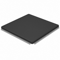
LPC2939FBD208,551 NXP Semiconductors, LPC2939FBD208,551 Datasheet - Page 44

LPC2939FBD208,551
Manufacturer Part Number
LPC2939FBD208,551
Description
IC ARM9 MCU FLASH 768KB 208-LQFP
Manufacturer
NXP Semiconductors
Series
LPC2900r
Datasheet
1.LPC2939FBD208551.pdf
(99 pages)
Specifications of LPC2939FBD208,551
Core Processor
ARM9
Core Size
32-Bit
Speed
125MHz
Connectivity
CAN, EBI/EMI, I²C, LIN, SPI, UART/USART, USB, USB OTG
Peripherals
DMA, POR, PWM, WDT
Number Of I /o
152
Program Memory Size
768KB (768K x 8)
Program Memory Type
FLASH
Eeprom Size
16K x 8
Ram Size
56K x 8
Voltage - Supply (vcc/vdd)
1.71 V ~ 3.6 V
Data Converters
A/D 24x10b
Oscillator Type
Internal
Operating Temperature
-40°C ~ 85°C
Package / Case
208-LQFP
Processor Series
LPC29
Core
ARM968E-S
3rd Party Development Tools
MDK-ARM, RL-ARM, ULINK2
Development Tools By Supplier
OM11027
Package
208LQFP
Device Core
ARM968E-S
Family Name
LPC2900
Operating Supply Voltage
1.8|3.3 V
Data Bus Width
16|32 Bit
Number Of Programmable I/os
160
Interface Type
CAN/I2C/LIN/QSPI/UART/USB
On-chip Adc
24-chx10-bit
Number Of Timers
6
For Use With
568-4787 - BOARD EVAL LPC2939
Lead Free Status / RoHS Status
Lead free / RoHS Compliant
Other names
935287113551
Available stocks
Company
Part Number
Manufacturer
Quantity
Price
Company:
Part Number:
LPC2939FBD208,551
Manufacturer:
NXP Semiconductors
Quantity:
10 000
NXP Semiconductors
LPC2939_3
Product data sheet
Fig 9.
APB system bus
ADC block diagram
IRQ compare
6.15.4.1 Functional description
6.15.4.2 Pin description
IRQ scan
The ADC block diagram,
functionality is divided into two major parts; one part running on the MSCSS Subsystem
clock, the other on the ADC clock. This split into two clock domains affects the behavior
from a system-level perspective. The actual analog-to-digital conversions take place in the
ADC clock domain, but system control takes place in the system clock domain.
A mechanism is provided to modify configuration of the ADC and control the moment at
which the updated configuration is transferred to the ADC domain.
The ADC clock is limited to 4.5 MHz maximum frequency and should always be lower
than or equal to the system clock frequency. To meet this constraint or to select the
desired lower sampling frequency, the clock generation unit provides a programmable
fractional system-clock divider dedicated to the ADC clock. Conversion rate is determined
by the ADC clock frequency divided by the number of resolution bits plus one. Accessing
ADC registers requires an enabled ADC clock, which is controllable via the clock
generation unit, see
Each ADC has four start inputs. Note that start 0 and start 2 are captured in the system
clock domain while start 1 and start 3 are captured in the ADC domain. The start inputs
are connected at MSCSS level, see
The three ADC modules in the MSCSS have the pins described below. The ADCx input
pins are combined with other functions on the port pins of the LPC2939. The VREFN and
VREFP pins are common to all ADCs.
start 0
REGISTERS
system clock
CONTROL
ADC
AND
start 2
SYSTEM DOMAIN
configuration data
conversion data
All information provided in this document is subject to legal disclaimers.
update
IRQ
Section
Rev. 03 — 7 April 2010
Figure
6.16.2.
start 1
(up to 4.5 MHz)
REGISTERS
CONTROL
ADC clock
9, shows the basic architecture of each ADC. The ADC
ADC
AND
Section 6.15
start 3
Table 23
ARM9 microcontroller with CAN, LIN, and USB
sync_out
3.3 V
ADC DOMAIN
ADC1/2
shows the ADC pins.
3.3 V
for details.
ADC0
5 V
ANALOG
ANALOG
3.3 V IN
5 V IN
MUX
MUX
LPC2939
© NXP B.V. 2010. All rights reserved.
ADC0 IN[7:0]
ADC1 IN[7:0]
ADC2 IN[7:0]
002aae360
44 of 99


