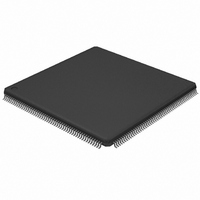
LPC2939FBD208,551 NXP Semiconductors, LPC2939FBD208,551 Datasheet - Page 58

LPC2939FBD208,551
Manufacturer Part Number
LPC2939FBD208,551
Description
IC ARM9 MCU FLASH 768KB 208-LQFP
Manufacturer
NXP Semiconductors
Series
LPC2900r
Datasheet
1.LPC2939FBD208551.pdf
(99 pages)
Specifications of LPC2939FBD208,551
Core Processor
ARM9
Core Size
32-Bit
Speed
125MHz
Connectivity
CAN, EBI/EMI, I²C, LIN, SPI, UART/USART, USB, USB OTG
Peripherals
DMA, POR, PWM, WDT
Number Of I /o
152
Program Memory Size
768KB (768K x 8)
Program Memory Type
FLASH
Eeprom Size
16K x 8
Ram Size
56K x 8
Voltage - Supply (vcc/vdd)
1.71 V ~ 3.6 V
Data Converters
A/D 24x10b
Oscillator Type
Internal
Operating Temperature
-40°C ~ 85°C
Package / Case
208-LQFP
Processor Series
LPC29
Core
ARM968E-S
3rd Party Development Tools
MDK-ARM, RL-ARM, ULINK2
Development Tools By Supplier
OM11027
Package
208LQFP
Device Core
ARM968E-S
Family Name
LPC2900
Operating Supply Voltage
1.8|3.3 V
Data Bus Width
16|32 Bit
Number Of Programmable I/os
160
Interface Type
CAN/I2C/LIN/QSPI/UART/USB
On-chip Adc
24-chx10-bit
Number Of Timers
6
For Use With
568-4787 - BOARD EVAL LPC2939
Lead Free Status / RoHS Status
Lead free / RoHS Compliant
Other names
935287113551
Available stocks
Company
Part Number
Manufacturer
Quantity
Price
Company:
Part Number:
LPC2939FBD208,551
Manufacturer:
NXP Semiconductors
Quantity:
10 000
NXP Semiconductors
LPC2939_3
Product data sheet
6.16.4.1 Functional description
6.16.4.2 Pin description
Each reset output is defined as a combination of reset input sources including the external
reset input pins and internal power-on reset, see
this table form a sort of cascade to provide the multiple levels of impact that a reset may
have. The combined input sources are logically OR-ed together so that activating any of
the listed reset sources causes the output to go active.
Table 30.
The RGU module in the LPC2939 has the following pins.
Reset output
POR_RST
RGU_RST
PCR_RST
COLD_RST
WARM_RST
SCU_RST
CFID_RST
FMC_RST
EMC_RST
SMC_RST
GESS_A2V_RST
PESS_A2V_RST
GPIO_RST
UART_RST
TMR_RST
SPI_RST
IVNSS_A2V_RST
IVNSS_CAN_RST
IVNSS_LIN_RST
MSCSS_A2V_RST
MSCSS_PWM_RST
MSCSS_ADC_RST
MSCSS_TMR_RST
I2C_RST
QEI_RST
DMA_RST
USB_RST
VIC_RST
AHB_RST
•
•
Monitor function to trace resets back to source
Register write-protection mechanism to prevent unintentional resets
Reset output configuration
All information provided in this document is subject to legal disclaimers.
POR_RST, RST pin
PCR_RST
WARM_RST
WARM_RST
WARM_RST
WARM_RST
WARM_RST
WARM_RST
WARM_RST
WARM_RST
Reset source
power-on reset module
RGU_RST, WATCHDOG PCR internal; source for COLD_RST
COLD_RST
COLD_RST
COLD_RST
COLD_RST
COLD_RST
COLD_RST
WARM_RST
WARM_RST
WARM_RST
WARM_RST
WARM_RST
WARM_RST
WARM_RST
WARM_RST
WARM_RST
WARM_RST
WARM_RST
Rev. 03 — 7 April 2010
ARM9 microcontroller with CAN, LIN, and USB
RGU internal; source for PCR_RST
parts with COLD_RST as reset source below
parts with WARM_RST as reset source below
SCU
embedded Flash-Memory Controller (FMC)
embedded SRAM-Memory Controller
external Static-Memory Controller (SMC)
all GPIO modules
all UART modules
all Timer modules in PESS
all SPI modules
all CAN modules including Acceptance filter
all LIN modules
all PWM modules
all ADC modules
all Timer modules in MSCSS
all I
Quadrature encoder
USB controller
Vectored Interrupt Controller (VIC)
Parts of the device reset when activated
LP_OSC; source for RGU_RST
CFID
GeSS AHB-to-APB bridge
PeSS AHB-to-APB bridge
IVNSS AHB-to-APB bridge
MSCSS AHB to APB bridge
GPDMA controller
CPU and AHB Bus infrastructure
Table
2
C modules
30. The first five resets listed in
Table 31
shows the RGU pins.
LPC2939
© NXP B.V. 2010. All rights reserved.
58 of 99


