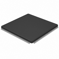
LPC2939FBD208,551 NXP Semiconductors, LPC2939FBD208,551 Datasheet - Page 38

LPC2939FBD208,551
Manufacturer Part Number
LPC2939FBD208,551
Description
IC ARM9 MCU FLASH 768KB 208-LQFP
Manufacturer
NXP Semiconductors
Series
LPC2900r
Datasheet
1.LPC2939FBD208551.pdf
(99 pages)
Specifications of LPC2939FBD208,551
Core Processor
ARM9
Core Size
32-Bit
Speed
125MHz
Connectivity
CAN, EBI/EMI, I²C, LIN, SPI, UART/USART, USB, USB OTG
Peripherals
DMA, POR, PWM, WDT
Number Of I /o
152
Program Memory Size
768KB (768K x 8)
Program Memory Type
FLASH
Eeprom Size
16K x 8
Ram Size
56K x 8
Voltage - Supply (vcc/vdd)
1.71 V ~ 3.6 V
Data Converters
A/D 24x10b
Oscillator Type
Internal
Operating Temperature
-40°C ~ 85°C
Package / Case
208-LQFP
Processor Series
LPC29
Core
ARM968E-S
3rd Party Development Tools
MDK-ARM, RL-ARM, ULINK2
Development Tools By Supplier
OM11027
Package
208LQFP
Device Core
ARM968E-S
Family Name
LPC2900
Operating Supply Voltage
1.8|3.3 V
Data Bus Width
16|32 Bit
Number Of Programmable I/os
160
Interface Type
CAN/I2C/LIN/QSPI/UART/USB
On-chip Adc
24-chx10-bit
Number Of Timers
6
For Use With
568-4787 - BOARD EVAL LPC2939
Lead Free Status / RoHS Status
Lead free / RoHS Compliant
Other names
935287113551
Available stocks
Company
Part Number
Manufacturer
Quantity
Price
Company:
Part Number:
LPC2939FBD208,551
Manufacturer:
NXP Semiconductors
Quantity:
10 000
NXP Semiconductors
LPC2939_3
Product data sheet
6.13.6.1 Functional description
6.13.6.2 Pin description
6.13.6.3 Clock description
6.14.1 CAN gateway
6.14 Networking subsystem
The general-purpose I/O provides individual control over each bidirectional port pin. There
are two registers to control I/O direction and output level. The inputs are synchronized to
achieve stable read levels.
To generate an open-drain output, set the bit in the output register to the desired value.
Use the direction register to control the signal. When set to output, the output driver
actively drives the value on the output; when set to input the signal floats and can be
pulled up internally or externally.
The six GPIO ports in the LPC2939 have the pins listed below. The GPIO pins are
combined with other functions on the port pins of the LPC2939.
pins.
Table 19.
The GPIO modules are clocked by several clocks, all of which are derived from
BASE_SYS_CLK; CLK_SYS_PESS and CLK_SYS_GPIOx (x = 0, 1, 2, 3, 4, 5), see
Section
power management. The frequency of all clocks CLK_SYS_GPIOx is identical to
CLK_SYS_PESS since they are derived from the same base clock BASE_SYS_CLK.
Controller Area Network (CAN) is the definition of a high-performance communication
protocol for serial data communication. The two CAN controllers in the LPC2939 provide a
full implementation of the CAN protocol according to the CAN specification version 2.0B.
The gateway concept is fully scalable with the number of CAN controllers, and always
operates together with a separate powerful and flexible hardware acceptance filter.
The key features are:
Symbol
GPIO0 pin[31:0]
GPIO1 pin[31:0]
GPIO2 pin[27:0]
GPIO3 pin[15:0]
GPIO4 pin[23:0]
GPIO5 pin[19:0]
•
•
•
•
•
•
All I/O pins default to input at reset to avoid any possible bus conflicts
Supports 11-bit as well as 29-bit identifiers
Double receive buffer and triple transmit buffer
Programmable error-warning limit and error counters with read/write access
Arbitration-lost capture and error-code capture with detailed bit position
Single-shot transmission (i.e. no re-transmission)
6.7.2. Note that each GPIO has its own CLK__SYS_GPIOx branch clock for
GPIO pins
All information provided in this document is subject to legal disclaimers.
Pin name
P0[31:0]
P1[31:0]
P2[27:0]
P3[15:0]
P4[23:0]
P5[19:0]
Rev. 03 — 7 April 2010
Direction
IN/OUT
IN/OUT
IN/OUT
IN/OUT
IN/OUT
IN/OUT
ARM9 microcontroller with CAN, LIN, and USB
Description
GPIO port x pins 31 to 0
GPIO port x pins 31 to 0
GPIO port x pins 27 to 0
GPIO port x pins 15 to 0
GPIO port x pins 23 to 0
GPIO port x pins 19 to 0
Table 19
LPC2939
© NXP B.V. 2010. All rights reserved.
shows the GPIO
38 of 99


