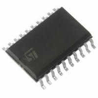
ST7FDALIF2M6 STMicroelectronics, ST7FDALIF2M6 Datasheet - Page 62

ST7FDALIF2M6
Manufacturer Part Number
ST7FDALIF2M6
Description
IC MCU 8BIT 8K 20-SOIC
Manufacturer
STMicroelectronics
Series
ST7r
Datasheet
1.ST7DALI-EVAL.pdf
(171 pages)
Specifications of ST7FDALIF2M6
Core Processor
ST7
Core Size
8-Bit
Speed
8MHz
Connectivity
DALI, SPI
Peripherals
LVD, POR, PWM, WDT
Number Of I /o
15
Program Memory Size
8KB (8K x 8)
Program Memory Type
FLASH
Eeprom Size
256 x 8
Ram Size
384 x 8
Voltage - Supply (vcc/vdd)
2.4 V ~ 5.5 V
Data Converters
A/D 7x10b
Oscillator Type
Internal
Operating Temperature
-40°C ~ 85°C
Package / Case
20-SOIC (7.5mm Width)
Processor Series
ST7DALI
Core
ST7
Data Bus Width
8 bit
Data Ram Size
384 B
Interface Type
DALI, SPI
Maximum Clock Frequency
8 MHz
Number Of Programmable I/os
15
Number Of Timers
4 bit
Operating Supply Voltage
2.4 V to 5.5 V
Maximum Operating Temperature
+ 85 C
Mounting Style
SMD/SMT
Development Tools By Supplier
ST7FLITE-SK/RAIS, ST7DALI-EVAL, ST7MDT10-DVP3, ST7MDT10-EMU3, STX-RLINK
Minimum Operating Temperature
- 40 C
On-chip Adc
8 bit
For Use With
497-5046 - KIT TOOL FOR ST7/UPSD/STR7 MCU
Lead Free Status / RoHS Status
Lead free / RoHS Compliant
Other names
497-2131-5
Available stocks
Company
Part Number
Manufacturer
Quantity
Price
Company:
Part Number:
ST7FDALIF2M6TR
Manufacturer:
NEC
Quantity:
670
I/O ports
Caution:
12.2.2
62/171
When enabling/disabling an external interrupt by setting/resetting the related OR register bit,
a spurious interrupt is generated if the pin level is low and its edge sensitivity includes
falling/rising edge. This is due to the edge detector input which is switched to '1' when the
external interrupt is disabled by the OR register.
To avoid this unwanted interrupt, a "safe" edge sensitivity (rising edge for enabling and
falling edge for disabling) has to be selected before changing the OR register bit and
configuring the appropriate sensitivity again.
In case a pin level change occurs during these operations (asynchronous signal input), as
interrupts are generated according to the current sensitivity, it is advised to disable all
interrupts before and to reenable them after the complete previous sequence in order to
avoid an external interrupt occurring on the unwanted edge.
This corresponds to the following steps:
1. To enable an external interrupt:
2. To disable an external interrupt:
Output modes
Setting the DDRx bit selects output mode. Writing to the DR bits applies a digital value to the
I/O through the latch. Reading the DR bits returns the previously stored value.
If an OR bit is available, different output modes can be selected by software: push-pull or
open-drain. Refer to I/O Port Implementation section for configuration.
Table 24.
– set the interrupt mask with the SIM instruction (in cases where a pin level change
– select rising edge
– enable the external interrupt through the OR register
– select the desired sensitivity if different from rising edge
– reset the interrupt mask with the RIM instruction (in cases where a pin level change
– set the interrupt mask with the SIM instruction SIM (in cases where a pin level change
– select falling edge
– disable the external interrupt through the OR register
– select rising edge
– reset the interrupt mask with the RIM instruction (in cases where a pin level change
could occur)
could occur)
could occur)
could occur)
DR
0
1
DR value and output pin status
Push-pull
V
V
OH
OL
Open-drain
Floating
V
OL
ST7DALIF2


