MC9S08SL16CTL Freescale Semiconductor, MC9S08SL16CTL Datasheet - Page 15
MC9S08SL16CTL
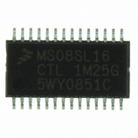
Manufacturer Part Number
MC9S08SL16CTL
Description
MCU 16KB FLASH SLIC 28TSSOP
Manufacturer
Freescale Semiconductor
Series
HCS08r
Datasheet
1.DEMO9S08EL32.pdf
(356 pages)
Specifications of MC9S08SL16CTL
Core Processor
HCS08
Core Size
8-Bit
Speed
40MHz
Connectivity
I²C, LIN, SCI, SPI
Peripherals
LVD, POR, PWM, WDT
Number Of I /o
22
Program Memory Size
16KB (16K x 8)
Program Memory Type
FLASH
Eeprom Size
256 x 8
Ram Size
512 x 8
Voltage - Supply (vcc/vdd)
2.7 V ~ 5.5 V
Data Converters
A/D 16x10b
Oscillator Type
External
Operating Temperature
-40°C ~ 85°C
Package / Case
28-TSSOP
Processor Series
S08SL
Core
HCS08
Data Bus Width
8 bit
Data Ram Size
512 B
Interface Type
I2C/SCI/SPI
Maximum Clock Frequency
40 MHz
Number Of Programmable I/os
22
Number Of Timers
6
Operating Supply Voltage
5.5 V
Maximum Operating Temperature
+ 85 C
Mounting Style
SMD/SMT
3rd Party Development Tools
EWS08
Development Tools By Supplier
DEMO9S08EL32, DEMO9S08EL32AUTO
Minimum Operating Temperature
- 40 C
On-chip Adc
16-ch x 10-bit
Package
28TSSOP
Family Name
HCS08
Maximum Speed
40 MHz
For Use With
DEMO9S08EL32 - BOARD DEMO FOR 9S08 EL MCUDEMO9S08EL32AUTO - DEMO BOARD EL32 AUTO
Lead Free Status / RoHS Status
Lead free / RoHS Compliant
Available stocks
Company
Part Number
Manufacturer
Quantity
Price
Company:

Part Number:
MC9S08SL16CTL
Manufacturer:
Freescale
Quantity:
2 359


Section Number
13.1 Introduction ...................................................................................................................................233
13.2 External Signal Description ..........................................................................................................238
13.3 Modes of Operation .......................................................................................................................239
13.4 Register Definition ........................................................................................................................239
13.5 Functional Description ..................................................................................................................244
14.1 Introduction ...................................................................................................................................249
14.2 Register Definition ........................................................................................................................254
Freescale Semiconductor
12.6.16Byte Transfer Mode Operation .......................................................................................224
12.6.17Oscillator Trimming with SLIC ......................................................................................228
12.6.18Digital Receive Filter ......................................................................................................230
13.1.1 Features ...........................................................................................................................235
13.1.2 Block Diagrams ..............................................................................................................235
13.1.3 SPI Baud Rate Generation ..............................................................................................237
13.2.1 SPSCK — SPI Serial Clock ............................................................................................238
13.2.2 MOSI — Master Data Out, Slave Data In ......................................................................238
13.2.3 MISO — Master Data In, Slave Data Out ......................................................................238
13.2.4 SS — Slave Select ..........................................................................................................238
13.3.1 SPI in Stop Modes ..........................................................................................................239
13.4.1 SPI Control Register 1 (SPIC1) ......................................................................................239
13.4.2 SPI Control Register 2 (SPIC2) ......................................................................................240
13.4.3 SPI Baud Rate Register (SPIBR) ....................................................................................241
13.4.4 SPI Status Register (SPIS) ..............................................................................................242
13.4.5 SPI Data Register (SPID) ...............................................................................................243
13.5.1 SPI Clock Formats ..........................................................................................................244
13.5.2 SPI Interrupts ..................................................................................................................247
13.5.3 Mode Fault Detection .....................................................................................................247
14.1.1 Features ...........................................................................................................................251
14.1.2 Modes of Operation ........................................................................................................251
14.1.3 Block Diagram ................................................................................................................252
14.2.1 SCI Baud Rate Registers (SCIxBDH, SCIxBDL) ..........................................................254
14.2.2 SCI Control Register 1 (SCIxC1) ...................................................................................255
14.2.3 SCI Control Register 2 (SCIxC2) ...................................................................................256
14.2.4 SCI Status Register 1 (SCIxS1) ......................................................................................257
14.2.5 SCI Status Register 2 (SCIxS2) ......................................................................................259
14.2.6 SCI Control Register 3 (SCIxC3) ...................................................................................260
14.2.7 SCI Data Register (SCIxD) .............................................................................................261
Serial Communications Interface (S08SCIV4)
MC9S08EL32 Series and MC9S08SL16 Series Data Sheet, Rev. 3
Serial Peripheral Interface (S08SPIV3)
Chapter 13
Chapter 14
Title
Page
15
Related parts for MC9S08SL16CTL
Image
Part Number
Description
Manufacturer
Datasheet
Request
R

Part Number:
Description:
Manufacturer:
Freescale Semiconductor, Inc
Datasheet:
Part Number:
Description:
Manufacturer:
Freescale Semiconductor, Inc
Datasheet:
Part Number:
Description:
Manufacturer:
Freescale Semiconductor, Inc
Datasheet:
Part Number:
Description:
Manufacturer:
Freescale Semiconductor, Inc
Datasheet:
Part Number:
Description:
Manufacturer:
Freescale Semiconductor, Inc
Datasheet:
Part Number:
Description:
Manufacturer:
Freescale Semiconductor, Inc
Datasheet:
Part Number:
Description:
Manufacturer:
Freescale Semiconductor, Inc
Datasheet:
Part Number:
Description:
Manufacturer:
Freescale Semiconductor, Inc
Datasheet:
Part Number:
Description:
Manufacturer:
Freescale Semiconductor, Inc
Datasheet:
Part Number:
Description:
Manufacturer:
Freescale Semiconductor, Inc
Datasheet:
Part Number:
Description:
Manufacturer:
Freescale Semiconductor, Inc
Datasheet:
Part Number:
Description:
Manufacturer:
Freescale Semiconductor, Inc
Datasheet:
Part Number:
Description:
Manufacturer:
Freescale Semiconductor, Inc
Datasheet:
Part Number:
Description:
Manufacturer:
Freescale Semiconductor, Inc
Datasheet:
Part Number:
Description:
Manufacturer:
Freescale Semiconductor, Inc
Datasheet: