DF2210CUNP24V Renesas Electronics America, DF2210CUNP24V Datasheet - Page 498
DF2210CUNP24V
Manufacturer Part Number
DF2210CUNP24V
Description
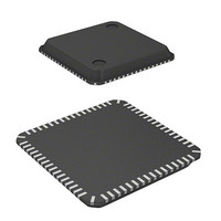
MCU 16BIT FLASH 3V 32K 64-QFN
Manufacturer
Renesas Electronics America
Series
H8® H8S/2200r
Datasheet
1.DF2218UTF24V.pdf
(758 pages)
Specifications of DF2210CUNP24V
Core Processor
H8S/2000
Core Size
16-Bit
Speed
24MHz
Connectivity
SCI, SmartCard, USB
Peripherals
DMA, POR, PWM, WDT
Number Of I /o
37
Program Memory Size
32KB (32K x 8)
Program Memory Type
FLASH
Ram Size
4K x 8
Voltage - Supply (vcc/vdd)
2.7 V ~ 3.6 V
Data Converters
A/D 6x10b
Oscillator Type
External
Operating Temperature
-20°C ~ 75°C
Package / Case
64-QFN
Lead Free Status / RoHS Status
Lead free / RoHS Compliant
Eeprom Size
-
Available stocks
Company
Part Number
Manufacturer
Quantity
Price
Company:

Part Number:
DF2210CUNP24V
Manufacturer:
Renesas Electronics America
Quantity:
135


12.10.3 Mark State and Break Detection (Asynchronous Mode Only)
When TE is 0, the TxD pin is used as an I/O port whose direction (input or output) and level are
determined by DR and DDR. This can be used to set the TxD pin to mark state (high level) or send
a break during serial data transmission. To maintain the communication line at mark state until TE
is set to 1, set both DDR and DR to 1. As TE is cleared to 0 at this point, the TxD pin becomes an
I/O port, and 1 is output from the TxD pin. To send a break during serial transmission, first set
PCR to 1 and PDR to 0, and then clear TE to 0. When TE is cleared to 0, the transmitter is
initialized regardless of the current transmission state, the TxD pin becomes an I/O port, and 0 is
output from the TxD pin.
12.10.4 Receive Error Flags and Transmit Operations (Clocked Synchronous Mode Only)
Transmission cannot be started when a receive error flag (ORER, PER, or FER) is set to 1, even if
the TDRE flag is cleared to 0. Be sure to clear the receive error flags to 0 before starting
transmission. Note also that receive error flags cannot be cleared to 0 even if the RE bit is cleared
to 0.
12.10.5 Restrictions on Use of DMAC
• When an external clock source is used as the serial clock, the transmit clock should not be
• When RDR is read by the DMAC, be sure to set the activation source to the relevant SCI
Rev.7.00 Dec. 24, 2008 Page 442 of 698
REJ09B0074-0700
input until at least 5 φ clock cycles after TDR is updated by the DMAC. Misoperation may
occur if the transmit clock is input within 4 φ clocks after TDR is updated. (figure 12.38)
SCK
TDRE
Serial data
Note: When operating on an external clock, set t>4 clocks.
reception end interrupt (RXI).
Figure 12.38 Example of Clocked Synchronous Transmission by DMAC
t
LSB
D0
D1
D2
D3
D4
D5
D6
D7
Related parts for DF2210CUNP24V
Image
Part Number
Description
Manufacturer
Datasheet
Request
R

Part Number:
Description:
KIT STARTER FOR M16C/29
Manufacturer:
Renesas Electronics America
Datasheet:

Part Number:
Description:
KIT STARTER FOR R8C/2D
Manufacturer:
Renesas Electronics America
Datasheet:

Part Number:
Description:
R0K33062P STARTER KIT
Manufacturer:
Renesas Electronics America
Datasheet:

Part Number:
Description:
KIT STARTER FOR R8C/23 E8A
Manufacturer:
Renesas Electronics America
Datasheet:

Part Number:
Description:
KIT STARTER FOR R8C/25
Manufacturer:
Renesas Electronics America
Datasheet:

Part Number:
Description:
KIT STARTER H8S2456 SHARPE DSPLY
Manufacturer:
Renesas Electronics America
Datasheet:

Part Number:
Description:
KIT STARTER FOR R8C38C
Manufacturer:
Renesas Electronics America
Datasheet:

Part Number:
Description:
KIT STARTER FOR R8C35C
Manufacturer:
Renesas Electronics America
Datasheet:

Part Number:
Description:
KIT STARTER FOR R8CL3AC+LCD APPS
Manufacturer:
Renesas Electronics America
Datasheet:
Part Number:
Description:
KIT STARTER FOR RX610
Manufacturer:
Renesas Electronics America
Datasheet:

Part Number:
Description:
KIT STARTER FOR R32C/118
Manufacturer:
Renesas Electronics America
Datasheet:

Part Number:
Description:
KIT DEV RSK-R8C/26-29
Manufacturer:
Renesas Electronics America
Datasheet:

Part Number:
Description:
KIT STARTER FOR SH7124
Manufacturer:
Renesas Electronics America
Datasheet:

Part Number:
Description:
KIT STARTER FOR H8SX/1622
Manufacturer:
Renesas Electronics America
Datasheet:

Part Number:
Description:
KIT DEV FOR SH7203
Manufacturer:
Renesas Electronics America
Datasheet: