MC908GT16CBE Freescale Semiconductor, MC908GT16CBE Datasheet - Page 40
MC908GT16CBE
Manufacturer Part Number
MC908GT16CBE
Description
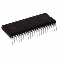
IC MCU 16K FLASH 8MHZ SPI 42SDIP
Manufacturer
Freescale Semiconductor
Series
HC08r
Datasheet
1.MC908GT8CFBE.pdf
(292 pages)
Specifications of MC908GT16CBE
Core Processor
HC08
Core Size
8-Bit
Speed
8MHz
Connectivity
SCI, SPI
Peripherals
LVD, POR, PWM
Number Of I /o
36
Program Memory Size
16KB (16K x 8)
Program Memory Type
FLASH
Ram Size
512 x 8
Voltage - Supply (vcc/vdd)
2.7 V ~ 5.5 V
Data Converters
A/D 8x8b
Oscillator Type
Internal
Operating Temperature
-40°C ~ 85°C
Package / Case
42-DIP (0.600", 15.24mm)
Controller Family/series
HC08
No. Of I/o's
34
Ram Memory Size
512Byte
Cpu Speed
8MHz
No. Of Timers
2
Embedded Interface Type
I2C, SCI, SPI
Rohs Compliant
Yes
Processor Series
HC08GT
Core
HC08
Data Bus Width
8 bit
Data Ram Size
512 B
Interface Type
SCI, SPI
Maximum Clock Frequency
8 MHz
Number Of Programmable I/os
30
Number Of Timers
4
Operating Supply Voltage
0 V to 5 V
Maximum Operating Temperature
+ 85 C
Mounting Style
Through Hole
Development Tools By Supplier
FSICEBASE, DEMO908GZ60E, M68CBL05CE, M68EML08GPGTE
Minimum Operating Temperature
- 40 C
On-chip Adc
8 bit, 8 Channel
Package
42SPDIP
Family Name
HC08
Maximum Speed
8 MHz
Lead Free Status / RoHS Status
Lead free / RoHS Compliant
Eeprom Size
-
Lead Free Status / Rohs Status
Details


Memory
2.5 Random-Access Memory (RAM)
Addresses $0040 through $023F are RAM locations. The location of the stack RAM is programmable.
The 16-bit stack pointer allows the stack to be anywhere in the 64-Kbyte memory space.
Within page zero are 192 bytes of RAM. Because the location of the stack RAM is programmable, all page
zero RAM locations can be used for I/O control and user data or code. When the stack pointer is moved
from its reset location at $00FF out of page zero, direct addressing mode instructions can efficiently
access all page zero RAM locations. Page zero RAM, therefore, provides ideal locations for frequently
accessed global variables.
Before processing an interrupt, the CPU uses five bytes of the stack to save the contents of the CPU
registers.
During a subroutine call, the CPU uses two bytes of the stack to store the return address. The stack
pointer decrements during pushes and increments during pulls.
2.6 Flash Memory
This sub-section describes the operation of the embedded Flash memory. This memory can be read,
programmed, and erased from a single external supply. The program, erase, and read operations are
enabled through the use of an internal charge pump.
2.6.1 Functional Description
The Flash memory is an array of 15,872 bytes (7,680 bytes on MC68HC908GT8) with an additional
36 bytes of user vectors, one byte of block protection and two bytes of ICG user trim storage. An erased
bit reads as 1 and a programmed bit reads as a 0. Memory in the Flash array is organized into two rows
per page basis. The page size is 64 bytes per page and the row size is 32 bytes per row. Hence the
minimum erase page size is 64 bytes and the minimum program row size is 32 bytes. Program and erase
operation operations are facilitated through control bits in Flash control register (FLCR). Details for these
operations appear later in this section.
The address ranges for the user memory and vectors are:
40
•
•
•
•
•
•
$C000–$FDFF; user memory ($E000–$FDFF on MC68HC908GT8)
$FE08
$FF7E; Flash block protect register
$FF80
$FF81
$FFDC–$FFFF; these locations are reserved for user-defined interrupt and reset vectors
;
;
;
ICG user trim register (ICGTR5)
ICG user trim register (ICGTR3)
Flash control register
For correct operation, the stack pointer must point only to RAM locations.
For M6805 compatibility, the H register is not stacked.
Be careful when using nested subroutines. The CPU may overwrite data in
the RAM during a subroutine or during the interrupt stacking operation.
MC68HC908GT16 • MC68HC908GT8 • MC68HC08GT16 Data Sheet, Rev. 5.0
NOTE
NOTE
NOTE
Freescale Semiconductor
Related parts for MC908GT16CBE
Image
Part Number
Description
Manufacturer
Datasheet
Request
R

Part Number:
Description:
Manufacturer:
Freescale Semiconductor, Inc
Datasheet:
Part Number:
Description:
Manufacturer:
Freescale Semiconductor, Inc
Datasheet:
Part Number:
Description:
Manufacturer:
Freescale Semiconductor, Inc
Datasheet:
Part Number:
Description:
Manufacturer:
Freescale Semiconductor, Inc
Datasheet:
Part Number:
Description:
Manufacturer:
Freescale Semiconductor, Inc
Datasheet:
Part Number:
Description:
Manufacturer:
Freescale Semiconductor, Inc
Datasheet:
Part Number:
Description:
Manufacturer:
Freescale Semiconductor, Inc
Datasheet:
Part Number:
Description:
Manufacturer:
Freescale Semiconductor, Inc
Datasheet:
Part Number:
Description:
Manufacturer:
Freescale Semiconductor, Inc
Datasheet:
Part Number:
Description:
Manufacturer:
Freescale Semiconductor, Inc
Datasheet:
Part Number:
Description:
Manufacturer:
Freescale Semiconductor, Inc
Datasheet:
Part Number:
Description:
Manufacturer:
Freescale Semiconductor, Inc
Datasheet:
Part Number:
Description:
Manufacturer:
Freescale Semiconductor, Inc
Datasheet:
Part Number:
Description:
Manufacturer:
Freescale Semiconductor, Inc
Datasheet:
Part Number:
Description:
Manufacturer:
Freescale Semiconductor, Inc
Datasheet: