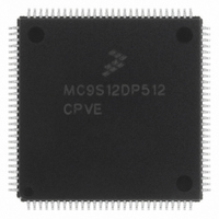
MC9S12DP512CPVER Freescale Semiconductor, MC9S12DP512CPVER Datasheet - Page 65

MC9S12DP512CPVER
Manufacturer Part Number
MC9S12DP512CPVER
Description
IC MCU 16BIT 4K FLASH 112-LQFP
Manufacturer
Freescale Semiconductor
Series
HCS12r
Datasheet
1.MC9S12DP512CPVE.pdf
(124 pages)
Specifications of MC9S12DP512CPVER
Core Processor
HCS12
Core Size
16-Bit
Speed
25MHz
Connectivity
CAN, I²C, SCI, SPI
Peripherals
PWM, WDT
Number Of I /o
91
Program Memory Size
512KB (512K x 8)
Program Memory Type
FLASH
Eeprom Size
4K x 8
Ram Size
12K x 8
Voltage - Supply (vcc/vdd)
2.35 V ~ 5.25 V
Data Converters
A/D 16x10b
Oscillator Type
Internal
Operating Temperature
-40°C ~ 85°C
Package / Case
112-LQFP
Package
112LQFP
Family Name
HCS12
Maximum Speed
25 MHz
Operating Supply Voltage
2.5|5 V
Data Bus Width
16 Bit
Interface Type
CAN/I2C/SCI/SPI
On-chip Adc
2(8-chx10-bit)
Number Of Timers
8
Lead Free Status / RoHS Status
Lead free / RoHS Compliant
Other names
MC9S12DP512CPVERTR
Available stocks
Company
Part Number
Manufacturer
Quantity
Price
Company:
Part Number:
MC9S12DP512CPVER
Manufacturer:
Freescale Semiconductor
Quantity:
10 000
2.4.1 VDDX,VSSX — Power & Ground Pins for I/O Drivers
External power and ground for I/O drivers. Because fast signal transitions place high, short-duration
current demands on the power supply, use bypass capacitors with high-frequency characteristics and place
them as close to the MCU as possible. Bypass requirements depend on how heavily the MCU pins are
loaded.
2.4.2 VDDR, VSSR — Power & Ground Pins for I/O Drivers & Internal Voltage
Regulator
transitions place high, short-duration current demands on the power supply, use bypass capacitors with
high-frequency characteristics and place them as close to the MCU as possible. Bypass requirements
depend on how heavily the MCU pins are loaded.
2.4.3 VDD1, VDD2, VSS1, VSS2 — Internal Logic Power Supply Pins
Power is supplied to the MCU through VDD and VSS. Because fast signal transitions place high,
short-duration current demands on the power supply, use bypass capacitors with high-frequency
characteristics and place them as close to the MCU as possible. This 2.5V supply is derived from the
internal voltage regulator. There is no static load on those pins allowed. The internal voltage regulator is
turned off, if VREGEN is tied to ground.
2.4.4 VDDA, VSSA — Power Supply Pins for ATD and VREG
VDDA, VSSA are the power supply and ground input pins for the voltage regulator and the analog to
digital converter. It also provides the reference for the internal voltage regulator. This allows the supply
voltage to the ATD and the reference voltage to be bypassed independently.
2.4.5 VRH, VRL — ATD Reference Voltage Input Pins
VRH and VRL are the reference voltage input pins for the analog to digital converter.
2.4.6 VDDPLL, VSSPLL — Power Supply Pins for PLL
Provides operating voltage and ground for the Oscillator and the Phased-Locked Loop. This allows the
supply voltage to the Oscillator and PLL to be bypassed independently. This 2.5V voltage is generated by
the internal voltage regulator.
External power and ground for I/O drivers and input to the internal voltage regulator. Because fast signal
NOTE:
NOTE:
NOTE:
All VSS pins must be connected together in the application.
No load allowed except for bypass capacitors.
No load allowed except for bypass capacitors.
MC9S12DP512 Device Guide V01.25
65


