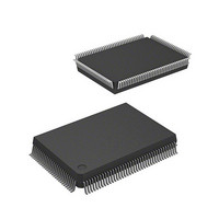
D12350F20IV Renesas Electronics America, D12350F20IV Datasheet - Page 18

D12350F20IV
Manufacturer Part Number
D12350F20IV
Description
IC H8S/2350 MCU 4.5/5.5V 0+K I-T
Manufacturer
Renesas Electronics America
Series
H8® H8S/2300r
Specifications of D12350F20IV
Core Processor
H8S/2000
Core Size
16-Bit
Speed
20MHz
Connectivity
SCI, SmartCard
Peripherals
DMA, POR, PWM, WDT
Number Of I /o
87
Program Memory Type
ROMless
Ram Size
2K x 8
Voltage - Supply (vcc/vdd)
2.7 V ~ 5.5 V
Data Converters
A/D 8x10b; D/A 2x8b
Oscillator Type
Internal
Operating Temperature
-40°C ~ 85°C
Package / Case
128-QFP
Lead Free Status / RoHS Status
Lead free / RoHS Compliant
Eeprom Size
-
Program Memory Size
-
Available stocks
Company
Part Number
Manufacturer
Quantity
Price
Company:
Part Number:
D12350F20IV
Manufacturer:
INF
Quantity:
4 834
- Current page: 18 of 1027
- Download datasheet (6Mb)
Rev. 3.00 Sep 15, 2006 page xvi of xxxiv
Item
B.2 Functions
C.13 Port G Block
Diagram
Figure C.13 (c-2)
H8S/2350 Port G Block
Diagram (Pin PG4)
D.2 Port States in Each
Mode [H8S/2350]
Table D.2 I/O Port
States in Each
Processing State
(H8S/2350)
Page
846
923
924
975
980
981
982
Revision (See Manual for Details)
Figure amended
BCRL H'FED5 Bus Controller
Figure amended
TMDR1 H'FFE1 TPU1
(Before) 1 Phase counting mode 4
mode 4
Figure amended
TIORL H'FFE2 TPU1
Figure C.13 (c-2) amended
Mode 1/2/4/5/6
Description in MCU operating mode in table D.2 amended
Port D 1, 4, 5
PF
PG
DACK Timing Select
TGR1B I/O Control
Legend: *: Don’t care
0
1
0
1
0
0
/BREQ 1, 4, 5
/CAS (Before) 1 to 3, 7
When DMAC single address transfer is performed in
DRAM space, full access is always executed DACK
signal goes low from T
Burst access is possible when DMAC single address
transfer is performed in DRAM space DACK signal
goes low from T
0
1
0
1
0
1
0
1
0
1
*
0
1
0
1
0
1
0
1
0
1
*
*
TGR1B
is output
compare
register
TGR1B
is input
capture
register
c1
or T
r
2
or T
cycle
Output disabled
Initial output is
0 output
Output disabled
Initial output is
1 output
Capture input
source is
TIOCB 1 pin
Capture input
source is TGR0B
compare match/
input capture
1
cycle
0 output at compare match
1 output at compare match
Toggle output at compare match
0 output at compare match
1 output at compare match
Toggle output at compare match
Input capture at rising edge
Input capture at falling edge
Input capture at both edges
Input capture at generation of
TGR0B compare match/input
capture
(After) 1
(After) Phase counting
Related parts for D12350F20IV
Image
Part Number
Description
Manufacturer
Datasheet
Request
R

Part Number:
Description:
KIT STARTER FOR M16C/29
Manufacturer:
Renesas Electronics America
Datasheet:

Part Number:
Description:
KIT STARTER FOR R8C/2D
Manufacturer:
Renesas Electronics America
Datasheet:

Part Number:
Description:
R0K33062P STARTER KIT
Manufacturer:
Renesas Electronics America
Datasheet:

Part Number:
Description:
KIT STARTER FOR R8C/23 E8A
Manufacturer:
Renesas Electronics America
Datasheet:

Part Number:
Description:
KIT STARTER FOR R8C/25
Manufacturer:
Renesas Electronics America
Datasheet:

Part Number:
Description:
KIT STARTER H8S2456 SHARPE DSPLY
Manufacturer:
Renesas Electronics America
Datasheet:

Part Number:
Description:
KIT STARTER FOR R8C38C
Manufacturer:
Renesas Electronics America
Datasheet:

Part Number:
Description:
KIT STARTER FOR R8C35C
Manufacturer:
Renesas Electronics America
Datasheet:

Part Number:
Description:
KIT STARTER FOR R8CL3AC+LCD APPS
Manufacturer:
Renesas Electronics America
Datasheet:

Part Number:
Description:
KIT STARTER FOR RX610
Manufacturer:
Renesas Electronics America
Datasheet:

Part Number:
Description:
KIT STARTER FOR R32C/118
Manufacturer:
Renesas Electronics America
Datasheet:

Part Number:
Description:
KIT DEV RSK-R8C/26-29
Manufacturer:
Renesas Electronics America
Datasheet:

Part Number:
Description:
KIT STARTER FOR SH7124
Manufacturer:
Renesas Electronics America
Datasheet:

Part Number:
Description:
KIT STARTER FOR H8SX/1622
Manufacturer:
Renesas Electronics America
Datasheet:

Part Number:
Description:
KIT DEV FOR SH7203
Manufacturer:
Renesas Electronics America
Datasheet:


