MC9S12XDT256MAA Freescale Semiconductor, MC9S12XDT256MAA Datasheet - Page 1152
MC9S12XDT256MAA
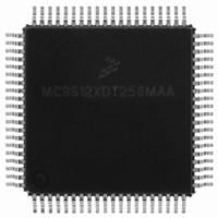
Manufacturer Part Number
MC9S12XDT256MAA
Description
IC MCU 256K FLASH 80-QFP
Manufacturer
Freescale Semiconductor
Series
HCS12r
Datasheet
1.MC9S12XD64CAA.pdf
(1348 pages)
Specifications of MC9S12XDT256MAA
Core Processor
HCS12X
Core Size
16-Bit
Speed
80MHz
Connectivity
CAN, EBI/EMI, I²C, IrDA, LIN, SCI, SPI
Peripherals
LVD, POR, PWM, WDT
Number Of I /o
59
Program Memory Size
256KB (256K x 8)
Program Memory Type
FLASH
Eeprom Size
4K x 8
Ram Size
16K x 8
Voltage - Supply (vcc/vdd)
2.35 V ~ 5.5 V
Data Converters
A/D 8x10b
Oscillator Type
External
Operating Temperature
-40°C ~ 125°C
Package / Case
80-QFP
Cpu Family
HCS12
Device Core Size
16b
Frequency (max)
40MHz
Interface Type
CAN/I2C/SCI/SPI
Total Internal Ram Size
16KB
# I/os (max)
59
Number Of Timers - General Purpose
12
Operating Supply Voltage (typ)
2.5/5V
Operating Supply Voltage (max)
2.75/5.5V
Operating Supply Voltage (min)
2.35/3.15V
On-chip Adc
8-chx10-bit
Instruction Set Architecture
CISC
Operating Temp Range
-40C to 125C
Operating Temperature Classification
Automotive
Mounting
Surface Mount
Pin Count
80
Package Type
PQFP
Processor Series
S12XD
Core
HCS12
Data Bus Width
16 bit
Data Ram Size
16 KB
Maximum Clock Frequency
40 MHz
Number Of Programmable I/os
59
Number Of Timers
12
Operating Supply Voltage
0 V to 5.5 V
Maximum Operating Temperature
+ 125 C
Mounting Style
SMD/SMT
3rd Party Development Tools
EWHCS12
Development Tools By Supplier
EVB9S12XDP512E
Minimum Operating Temperature
- 40 C
Lead Free Status / RoHS Status
Lead free / RoHS Compliant
Available stocks
Company
Part Number
Manufacturer
Quantity
Price

Company:
Part Number:
MC9S12XDT256MAA
Manufacturer:
Freescale Semiconductor
Quantity:
10 000


Chapter 28 256 Kbyte Flash Module (S12XFTX256K2V1)
28.3.2.1
The FCLKDIV register is used to control timed events in program and erase algorithms.
All bits in the FCLKDIV register are readable, bits 6-0 are write once and bit 7 is not writable.
28.3.2.2
The FSEC register holds all bits associated with the security of the MCU and Flash module.
1154
RESERVED1
RESERVED2
RESERVED3
RESERVED4
FDIV[5:0]
PRDIV8
FDIVLD
Register
Reset
Field
Name
5:0
7
6
W
R
FDIVLD
Clock Divider Loaded.
0 Register has not been written.
1 Register has been written to since the last reset.
Enable Prescalar by 8
0 The oscillator clock is directly fed into the clock divider
1 The oscillator clock is divided by 8 before feeding into the clock divider.
Clock Divider Bits — The combination of PRDIV8 and FDIV[5:0] must divide the oscillator clock down to a
frequency of 150 kHz–200 kHz. The maximum divide ratio is 512. Please refer to
FCLKDIV Register”
Flash Clock Divider Register (FCLKDIV)
Flash Security Register (FSEC)
0
7
W
W
W
W
R
R
R
R
Bit 7
= Unimplemented or Reserved
0
0
0
0
PRDIV8
Figure 28-3. FTX256K2 Register Summary (continued)
0
6
Figure 28-4. Flash Clock Divider Register (FCLKDIV)
for more information.
.
6
0
0
0
0
Table 28-2. FCLKDIV Field Descriptions
MC9S12XDP512 Data Sheet, Rev. 2.21
FDIV5
0
5
5
0
0
0
0
FDIV4
0
4
Description
4
0
0
0
0
.
FDIV3
0
3
3
0
0
0
0
FDIV2
0
2
2
0
0
0
0
Section 28.4.1.1, “Writing the
Freescale Semiconductor
FDIV1
0
1
1
0
0
0
0
FDIV0
Bit 0
0
0
0
0
0
0
Related parts for MC9S12XDT256MAA
Image
Part Number
Description
Manufacturer
Datasheet
Request
R

Part Number:
Description:
16-BIT MICROPROCESSOR FAMILY
Manufacturer:
FREESCALE [Freescale Semiconductor, Inc]
Datasheet:

Part Number:
Description:
Manufacturer:
Freescale Semiconductor, Inc
Datasheet:
Part Number:
Description:
Manufacturer:
Freescale Semiconductor, Inc
Datasheet:
Part Number:
Description:
Manufacturer:
Freescale Semiconductor, Inc
Datasheet:
Part Number:
Description:
Manufacturer:
Freescale Semiconductor, Inc
Datasheet:
Part Number:
Description:
Manufacturer:
Freescale Semiconductor, Inc
Datasheet:
Part Number:
Description:
Manufacturer:
Freescale Semiconductor, Inc
Datasheet:
Part Number:
Description:
Manufacturer:
Freescale Semiconductor, Inc
Datasheet:
Part Number:
Description:
Manufacturer:
Freescale Semiconductor, Inc
Datasheet:
Part Number:
Description:
Manufacturer:
Freescale Semiconductor, Inc
Datasheet:
Part Number:
Description:
Manufacturer:
Freescale Semiconductor, Inc
Datasheet:
Part Number:
Description:
Manufacturer:
Freescale Semiconductor, Inc
Datasheet:
Part Number:
Description:
Manufacturer:
Freescale Semiconductor, Inc
Datasheet:
Part Number:
Description:
Manufacturer:
Freescale Semiconductor, Inc
Datasheet:
Part Number:
Description:
Manufacturer:
Freescale Semiconductor, Inc
Datasheet: