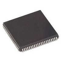
HD64F3337YCP16V Renesas Electronics America, HD64F3337YCP16V Datasheet - Page 530

HD64F3337YCP16V
Manufacturer Part Number
HD64F3337YCP16V
Description
MCU 3/5V 60K PB-FREE 84-PLCC
Manufacturer
Renesas Electronics America
Series
H8® H8/300r
Specifications of HD64F3337YCP16V
Core Size
8-Bit
Program Memory Size
60KB (60K x 8)
Oscillator Type
Internal
Core Processor
H8/300
Speed
16MHz
Connectivity
Host Interface, I²C, SCI
Peripherals
POR, PWM, WDT
Number Of I /o
74
Program Memory Type
FLASH
Ram Size
2K x 8
Voltage - Supply (vcc/vdd)
4.5 V ~ 5.5 V
Data Converters
A/D 8x10b; D/A 2x8b
Operating Temperature
-20°C ~ 75°C
Package / Case
84-PLCC
No. Of I/o's
74
Ram Memory Size
1KB
Cpu Speed
16MHz
No. Of Timers
6
No. Of Pwm Channels
2
Digital Ic Case Style
PLCC
Controller Family/series
H8/300
Rohs Compliant
Yes
Lead Free Status / RoHS Status
Lead free / RoHS Compliant
Eeprom Size
-
Lead Free Status / RoHS Status
Lead free / RoHS Compliant, Lead free / RoHS Compliant
Available stocks
Company
Part Number
Manufacturer
Quantity
Price
Company:
Part Number:
HD64F3337YCP16V
Manufacturer:
COILMASTER
Quantity:
30 000
Company:
Part Number:
HD64F3337YCP16V
Manufacturer:
Renesas Electronics America
Quantity:
10 000
- Current page: 530 of 747
- Download datasheet (4Mb)
Bits 1 and 0—Mode Select 1 and 0 (MDS1, MDS0): These bits indicate the input levels at mode
pins MD
and MD
pin (MD
21.1.7
Mode Transition Diagram: When the mode pins are set in the reset state and a reset start is
effected, the microcontroller enters one of the operating modes as shown in figure 21.2. In user
mode, the flash memory can be read but cannot be programmed or erased.
Modes in which the flash memory can be programmed and erased are boot mode, user
programming mode, and writer mode.
500
Notes: Transitions between user mode and user programming mode should only be made when the CPU is
FLSHE = 1
*1 MD
*2 MD
not accessing the flash memory.
0
with on-chip ROM
1
1
, respectively. MDS1 and MDS0 are read-only bits, and cannot be modified. The mode
Flash Memory Operating Modes
and MD
and MD
User mode
enabled
0
0
= MD
= MD
0
0
On-board programming mode
) input levels are latched into these bits when MDCR is read.
(the current operating mode). Bits MDS1 and MDS0 correspond to pins MD
programming
FLSHE = 0
1
1
Figure 21.2 Flash Memory Related State Transitions
= 0, P92 = P91 = P90 = 1
= 0, P92 = 0, P91 = P90 = 1
mode
User
MD
1
= 1
RES = 0
RES = 0
Reset state
Boot mode
*1
RES = 0
*2
RES = 0
Writer mode
1
Related parts for HD64F3337YCP16V
Image
Part Number
Description
Manufacturer
Datasheet
Request
R

Part Number:
Description:
KIT STARTER FOR M16C/29
Manufacturer:
Renesas Electronics America
Datasheet:

Part Number:
Description:
KIT STARTER FOR R8C/2D
Manufacturer:
Renesas Electronics America
Datasheet:

Part Number:
Description:
R0K33062P STARTER KIT
Manufacturer:
Renesas Electronics America
Datasheet:

Part Number:
Description:
KIT STARTER FOR R8C/23 E8A
Manufacturer:
Renesas Electronics America
Datasheet:

Part Number:
Description:
KIT STARTER FOR R8C/25
Manufacturer:
Renesas Electronics America
Datasheet:

Part Number:
Description:
KIT STARTER H8S2456 SHARPE DSPLY
Manufacturer:
Renesas Electronics America
Datasheet:

Part Number:
Description:
KIT STARTER FOR R8C38C
Manufacturer:
Renesas Electronics America
Datasheet:

Part Number:
Description:
KIT STARTER FOR R8C35C
Manufacturer:
Renesas Electronics America
Datasheet:

Part Number:
Description:
KIT STARTER FOR R8CL3AC+LCD APPS
Manufacturer:
Renesas Electronics America
Datasheet:

Part Number:
Description:
KIT STARTER FOR RX610
Manufacturer:
Renesas Electronics America
Datasheet:

Part Number:
Description:
KIT STARTER FOR R32C/118
Manufacturer:
Renesas Electronics America
Datasheet:

Part Number:
Description:
KIT DEV RSK-R8C/26-29
Manufacturer:
Renesas Electronics America
Datasheet:

Part Number:
Description:
KIT STARTER FOR SH7124
Manufacturer:
Renesas Electronics America
Datasheet:

Part Number:
Description:
KIT STARTER FOR H8SX/1622
Manufacturer:
Renesas Electronics America
Datasheet:

Part Number:
Description:
KIT DEV FOR SH7203
Manufacturer:
Renesas Electronics America
Datasheet:


