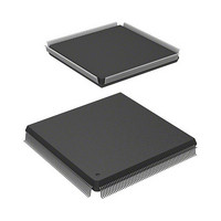
HD6417727F100V Renesas Electronics America, HD6417727F100V Datasheet - Page 171

HD6417727F100V
Manufacturer Part Number
HD6417727F100V
Description
MPU 3V 16K PB-FREE 240-QFP
Manufacturer
Renesas Electronics America
Series
SuperH® SH7700r
Datasheet
1.HD6417727BP100CV.pdf
(1098 pages)
Specifications of HD6417727F100V
Core Processor
SH-3 DSP
Core Size
32-Bit
Speed
100MHz
Connectivity
FIFO, SCI, SIO, SmartCard, USB
Peripherals
DMA, LCD, POR, WDT
Number Of I /o
104
Program Memory Type
ROMless
Ram Size
32K x 8
Voltage - Supply (vcc/vdd)
1.6 V ~ 2.05 V
Data Converters
A/D 6x10b; D/A 2x8b
Oscillator Type
Internal
Operating Temperature
-20°C ~ 75°C
Package / Case
240-QFP
Lead Free Status / RoHS Status
Lead free / RoHS Compliant
Eeprom Size
-
Program Memory Size
-
Available stocks
Company
Part Number
Manufacturer
Quantity
Price
Company:
Part Number:
HD6417727F100V
Manufacturer:
Renesas Electronics America
Quantity:
10 000
- Current page: 171 of 1098
- Download datasheet (7Mb)
3.4.4
When a 1-kbyte page is recorded in a TLB entry, a synonym problem may arise. If a number of
logical addresses are mapped onto a single physical address, the same physical address data will
be recorded in a number of cache entries, and it will not be possible to guarantee data congruity.
The reason why this problem only occurs when using a 1-kbyte page is explained below with
reference to figure 3.10.
To achieve high-speed operation of the SH7727 cache, an index number is created using logical
address bits 11 to 4. When a 4-kbyte page is used, logical address bits 11 to 4 are included in the
offset, and since they are not subject to address translation, they are the same as physical address
bits 11 to 4. In cache-based address comparison and recording in the address array, since the cache
tag address is a physical address, physical address bits 31 to 10 are recorded.
When a 1-kbyte page is used, also, a cache index number is created using logical address bits 11 to
4. However, in case of a 1-kbyte page, logical address bits 11 and 10 are subject to address
translation and therefore may not be the same as physical address bits 11 and 10. Consequently,
31
0
PTEH register
31
MMUCR
31
Avoiding Synonym Problems
Index
VPN(31−17)
VPN
0
17
9
SV 0 0 RC 0 TF IX AT
Figure 3.9 Operation of LDTLB Instruction
12
VPN(11−10)
Address array
Write
VPN
10 8
0
ASID
ASID(7−)
Way selection
0
0
V
Ways 0 to 3
Section 3 Memory Management Unit (MMU)
Rev.6.00 Mar. 27, 2009 Page 113 of 1036
PTEL register
PPN(31−10) PR(1−0) SZ C
31
PPN
10
Data array
0 V 0 PR SZ C D SH 0
Write
REJ09B0254-0600
D SH
0
Related parts for HD6417727F100V
Image
Part Number
Description
Manufacturer
Datasheet
Request
R

Part Number:
Description:
KIT STARTER FOR M16C/29
Manufacturer:
Renesas Electronics America
Datasheet:

Part Number:
Description:
KIT STARTER FOR R8C/2D
Manufacturer:
Renesas Electronics America
Datasheet:

Part Number:
Description:
R0K33062P STARTER KIT
Manufacturer:
Renesas Electronics America
Datasheet:

Part Number:
Description:
KIT STARTER FOR R8C/23 E8A
Manufacturer:
Renesas Electronics America
Datasheet:

Part Number:
Description:
KIT STARTER FOR R8C/25
Manufacturer:
Renesas Electronics America
Datasheet:

Part Number:
Description:
KIT STARTER H8S2456 SHARPE DSPLY
Manufacturer:
Renesas Electronics America
Datasheet:

Part Number:
Description:
KIT STARTER FOR R8C38C
Manufacturer:
Renesas Electronics America
Datasheet:

Part Number:
Description:
KIT STARTER FOR R8C35C
Manufacturer:
Renesas Electronics America
Datasheet:

Part Number:
Description:
KIT STARTER FOR R8CL3AC+LCD APPS
Manufacturer:
Renesas Electronics America
Datasheet:

Part Number:
Description:
KIT STARTER FOR RX610
Manufacturer:
Renesas Electronics America
Datasheet:

Part Number:
Description:
KIT STARTER FOR R32C/118
Manufacturer:
Renesas Electronics America
Datasheet:

Part Number:
Description:
KIT DEV RSK-R8C/26-29
Manufacturer:
Renesas Electronics America
Datasheet:

Part Number:
Description:
KIT STARTER FOR SH7124
Manufacturer:
Renesas Electronics America
Datasheet:

Part Number:
Description:
KIT STARTER FOR H8SX/1622
Manufacturer:
Renesas Electronics America
Datasheet:

Part Number:
Description:
KIT DEV FOR SH7203
Manufacturer:
Renesas Electronics America
Datasheet:


