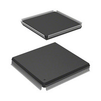
HD6417727F100V Renesas Electronics America, HD6417727F100V Datasheet - Page 846

HD6417727F100V
Manufacturer Part Number
HD6417727F100V
Description
MPU 3V 16K PB-FREE 240-QFP
Manufacturer
Renesas Electronics America
Series
SuperH® SH7700r
Datasheet
1.HD6417727BP100CV.pdf
(1098 pages)
Specifications of HD6417727F100V
Core Processor
SH-3 DSP
Core Size
32-Bit
Speed
100MHz
Connectivity
FIFO, SCI, SIO, SmartCard, USB
Peripherals
DMA, LCD, POR, WDT
Number Of I /o
104
Program Memory Type
ROMless
Ram Size
32K x 8
Voltage - Supply (vcc/vdd)
1.6 V ~ 2.05 V
Data Converters
A/D 6x10b; D/A 2x8b
Oscillator Type
Internal
Operating Temperature
-20°C ~ 75°C
Package / Case
240-QFP
Lead Free Status / RoHS Status
Lead free / RoHS Compliant
Eeprom Size
-
Program Memory Size
-
Available stocks
Company
Part Number
Manufacturer
Quantity
Price
Company:
Part Number:
HD6417727F100V
Manufacturer:
Renesas Electronics America
Quantity:
10 000
- Current page: 846 of 1098
- Download datasheet (7Mb)
Section 25 LCD Controller
Bits 1 and 0—LCD Module Power-Supply Input State (LPS1 and LPS0): Indicate the power-
supply input state of the LCD module when using the power-supply control function.
Bit 1
LPS1
0
1
25.2.18 LCDC Power-Supply Sequence Period Register (LDPSPR)
LDPSPR controls the power supply circuit that provides power to the LCD module. The timing to
start outputting the timing signals to the VEPWC and VCPWC pins is specified.
Bits 15 to 12—LCDC Power-On Sequence Period (ONA): Set the period from VCPWC
assertion to starting output of the display data (LCDD) and timing signals (FLM, CL1, CL2, and
M/DISP) in the power-on sequence of the LCD module in frame units.
This period is the (a) period in figures 25.4 to 25.7. 1 is to be subtracted from the setting.
Bits 11 to 8—LCDC Power-On Sequence Period (ONB): Set the period from starting output of
the display data (LCDD) and timing signals (FLM, CL1, CL2, and DISP/M) to the VEPWC
assertion in the power-on sequence of the LCD module in frame units.
This period is the (b) period in figures 25.4 to 25.7. 1 is to be subtracted from the setting.
Bits 7 to 4—LCDC Power-Off Sequence Period (OFFE): Set the period from VEPWC negation
to stopping output of the display data (LCDD) and timing signals (FLM, CL1, CL2, and DISP/M)
in the power-off sequence of the LCD module in frame units.
This period is the (e) period in figures 25.4 to 25.7. 1 is to be subtracted from the setting.
Bits 3 to 0—LCDC Power-Off Sequence Period (OFFF): Set the period from stopping output
of the display data (LCDD) and timing signals (FLM, CL1, CL2, and DISP/M) to VCPWC
negation to in the power-off sequence of the LCD module in frame units.
This period is the (f) period in figures 25.4 to 25.7. 1 is to be subtracted from the setting.
Rev.6.00 Mar. 27, 2009 Page 788 of 1036
REJ09B0254-0600
Initial value:
R/W:
Bit:
ONA3 ONA2 ONA1 ONA0 ONB3 ONB2 ONB1 ONB0 OFFE3 OFFE2 OFFE1 OFFE0 OFFF3 OFFF2 OFFF1 OFFF0
R/W
15
1
Bit 0
LPS0
0
1
R/W
14
1
R/W
13
1
Description
LCD module power off
LCD module power on
R/W
12
1
R/W
11
0
R/W
10
1
R/W
9
1
R/W
8
0
R/W
7
0
R/W
6
0
R/W
5
0
R/W
4
0
R/W
3
1
R/W
2
1
(Initial value)
R/W
1
1
R/W
0
1
Related parts for HD6417727F100V
Image
Part Number
Description
Manufacturer
Datasheet
Request
R

Part Number:
Description:
KIT STARTER FOR M16C/29
Manufacturer:
Renesas Electronics America
Datasheet:

Part Number:
Description:
KIT STARTER FOR R8C/2D
Manufacturer:
Renesas Electronics America
Datasheet:

Part Number:
Description:
R0K33062P STARTER KIT
Manufacturer:
Renesas Electronics America
Datasheet:

Part Number:
Description:
KIT STARTER FOR R8C/23 E8A
Manufacturer:
Renesas Electronics America
Datasheet:

Part Number:
Description:
KIT STARTER FOR R8C/25
Manufacturer:
Renesas Electronics America
Datasheet:

Part Number:
Description:
KIT STARTER H8S2456 SHARPE DSPLY
Manufacturer:
Renesas Electronics America
Datasheet:

Part Number:
Description:
KIT STARTER FOR R8C38C
Manufacturer:
Renesas Electronics America
Datasheet:

Part Number:
Description:
KIT STARTER FOR R8C35C
Manufacturer:
Renesas Electronics America
Datasheet:

Part Number:
Description:
KIT STARTER FOR R8CL3AC+LCD APPS
Manufacturer:
Renesas Electronics America
Datasheet:

Part Number:
Description:
KIT STARTER FOR RX610
Manufacturer:
Renesas Electronics America
Datasheet:

Part Number:
Description:
KIT STARTER FOR R32C/118
Manufacturer:
Renesas Electronics America
Datasheet:

Part Number:
Description:
KIT DEV RSK-R8C/26-29
Manufacturer:
Renesas Electronics America
Datasheet:

Part Number:
Description:
KIT STARTER FOR SH7124
Manufacturer:
Renesas Electronics America
Datasheet:

Part Number:
Description:
KIT STARTER FOR H8SX/1622
Manufacturer:
Renesas Electronics America
Datasheet:

Part Number:
Description:
KIT DEV FOR SH7203
Manufacturer:
Renesas Electronics America
Datasheet:


