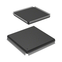
HD6417727F100V Renesas Electronics America, HD6417727F100V Datasheet - Page 360

HD6417727F100V
Manufacturer Part Number
HD6417727F100V
Description
MPU 3V 16K PB-FREE 240-QFP
Manufacturer
Renesas Electronics America
Series
SuperH® SH7700r
Datasheet
1.HD6417727BP100CV.pdf
(1098 pages)
Specifications of HD6417727F100V
Core Processor
SH-3 DSP
Core Size
32-Bit
Speed
100MHz
Connectivity
FIFO, SCI, SIO, SmartCard, USB
Peripherals
DMA, LCD, POR, WDT
Number Of I /o
104
Program Memory Type
ROMless
Ram Size
32K x 8
Voltage - Supply (vcc/vdd)
1.6 V ~ 2.05 V
Data Converters
A/D 6x10b; D/A 2x8b
Oscillator Type
Internal
Operating Temperature
-20°C ~ 75°C
Package / Case
240-QFP
Lead Free Status / RoHS Status
Lead free / RoHS Compliant
Eeprom Size
-
Program Memory Size
-
Available stocks
Company
Part Number
Manufacturer
Quantity
Price
Company:
Part Number:
HD6417727F100V
Manufacturer:
Renesas Electronics America
Quantity:
10 000
- Current page: 360 of 1098
- Download datasheet (7Mb)
Section 12 Bus State Controller (BSC)
Bits 4 and 3—Area 2 Wait Control (A2W1, A2W0): Specify the number of wait states inserted
into physical space area 2.
• For Ordinary memory
Bit 4: A2W0
0
1
• For Synchronous SDRAM
Bit 4: A2W1
0
1
Bits 2 to 0—Area 0 Wait Control (A0W2, A0W1, A0W0): Specify the number of wait states
inserted into physical space area 0. Also specify the burst pitch for burst transfer.
A0W2
0
1
Rev.6.00 Mar. 27, 2009 Page 302 of 1036
REJ09B0254-0600
Bit 2:
Bit 1:
A0W1
0
1
0
1
Bit 0:
A0W0
0
1
0
1
0
1
0
1
Bit 3: A2W0
0
1
0
1
Bit 3: A2W0
0
1
0
1
Inserted
Wait States
0
1
2
3
4
6
8
10
(Initial value)
First Cycle
Inserted Wait States
0
1
2
3
Description
Synchronous DRAM: CAS Latency
1
1
2
3
WAIT Pin
Ignored
Enable
Enable
Enable
Enable
Enable
Enable
Enable
Description
Number of States
Per Data Transfer WAIT Pin
2
2
3
4
4
6
8
10
Description
(Excluding First Cycle)
WAIT Pin
Ignored
Enable
Enable
Enable
Burst Cycle
Enable
Enable
Enable
Enable
Enable
Enable
Enable
Enable
(Initial value)
(Initial value)
Related parts for HD6417727F100V
Image
Part Number
Description
Manufacturer
Datasheet
Request
R

Part Number:
Description:
KIT STARTER FOR M16C/29
Manufacturer:
Renesas Electronics America
Datasheet:

Part Number:
Description:
KIT STARTER FOR R8C/2D
Manufacturer:
Renesas Electronics America
Datasheet:

Part Number:
Description:
R0K33062P STARTER KIT
Manufacturer:
Renesas Electronics America
Datasheet:

Part Number:
Description:
KIT STARTER FOR R8C/23 E8A
Manufacturer:
Renesas Electronics America
Datasheet:

Part Number:
Description:
KIT STARTER FOR R8C/25
Manufacturer:
Renesas Electronics America
Datasheet:

Part Number:
Description:
KIT STARTER H8S2456 SHARPE DSPLY
Manufacturer:
Renesas Electronics America
Datasheet:

Part Number:
Description:
KIT STARTER FOR R8C38C
Manufacturer:
Renesas Electronics America
Datasheet:

Part Number:
Description:
KIT STARTER FOR R8C35C
Manufacturer:
Renesas Electronics America
Datasheet:

Part Number:
Description:
KIT STARTER FOR R8CL3AC+LCD APPS
Manufacturer:
Renesas Electronics America
Datasheet:

Part Number:
Description:
KIT STARTER FOR RX610
Manufacturer:
Renesas Electronics America
Datasheet:

Part Number:
Description:
KIT STARTER FOR R32C/118
Manufacturer:
Renesas Electronics America
Datasheet:

Part Number:
Description:
KIT DEV RSK-R8C/26-29
Manufacturer:
Renesas Electronics America
Datasheet:

Part Number:
Description:
KIT STARTER FOR SH7124
Manufacturer:
Renesas Electronics America
Datasheet:

Part Number:
Description:
KIT STARTER FOR H8SX/1622
Manufacturer:
Renesas Electronics America
Datasheet:

Part Number:
Description:
KIT DEV FOR SH7203
Manufacturer:
Renesas Electronics America
Datasheet:


