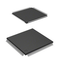
DF2166VTE33 Renesas Electronics America, DF2166VTE33 Datasheet - Page 152

DF2166VTE33
Manufacturer Part Number
DF2166VTE33
Description
MCU FLASH 3V 512K 33MHZ 144TQFP
Manufacturer
Renesas Electronics America
Series
H8® H8S/2100r
Datasheet
1.HS2168EPI61H-U.pdf
(876 pages)
Specifications of DF2166VTE33
Core Processor
H8S/2000
Core Size
16-Bit
Speed
33MHz
Connectivity
I²C, IrDA, LPC, SCI, SmartCard
Peripherals
POR, PWM, WDT
Number Of I /o
106
Program Memory Size
512KB (512K x 8)
Program Memory Type
FLASH
Ram Size
40K x 8
Voltage - Supply (vcc/vdd)
3 V ~ 3.6 V
Data Converters
A/D 8x10b; D/A 2x8b
Oscillator Type
External
Operating Temperature
-20°C ~ 75°C
Package / Case
144-TQFP, 144-VQFP
Lead Free Status / RoHS Status
Contains lead / RoHS non-compliant
Eeprom Size
-
- Current page: 152 of 876
- Download datasheet (5Mb)
6.3.4
WSCR2 is used to specify the wait mode and number of wait states in access to the 256-kbyte
extended area and CP extended area.
Bit
7
6
5
4
3
Rev. 3.00, 03/04, page 110 of 830
Bit Name
WMS10
WC11
WC10
WMS21
WMS20
Wait State Control Register 2 (WSCR2)
Initial
Value
0
1
1
0
0
R/W
R/W
R/W
R/W
R/W
R/W
Description
256-kbyte Extended Area Wait Mode Select 0
Selects the wait mode for access to the 256-kbyte extended
area when the CS256E bit in SYSCR and the AST256 bit in
WSCR are set to 1.
0: Program wait mode
1: Wait disabled mode
256-kbyte Extended Area Wait Count 1 and 0
Selects the number of program wait states to be inserted into
the data cycle for access to the 256-kbyte extended area
when the CS256E bit in SYSCR and the AST256 bit in WSCR
are set to 1.
00: Program wait state is not inserted
01: 1 program wait state is inserted
10: 2 program wait states are inserted
11: 3 program wait states are inserted
CP Extended Area Wait Mode Select 1 and 0
Selects the wait mode for access to the CP extended area
when the CPCSE and ASTCP bits in BCR2 are set to 1.
00: Program wait mode
01: Wait disabled mode
10: Pin wait mode
11: Pin auto-wait mode
Related parts for DF2166VTE33
Image
Part Number
Description
Manufacturer
Datasheet
Request
R

Part Number:
Description:
0.6mm Pitch Board-to-Fine-Coaxial Cable Connectors
Manufacturer:
Hirose Electric
Datasheet:

Part Number:
Description:
0.6mm Pitch Board-to-fine-coaxial Cable Connectors
Manufacturer:
Hirose Electric
Datasheet:

Part Number:
Description:
0.6mm Pitch Board-to-fine-coaxial Cable Connectors
Manufacturer:
Hirose Electric
Datasheet:

Part Number:
Description:
Right angle, Two-piece for fine coaxial cable, Discrete wire connectors; HRS No: 687-0001-5 56; No. of Positions: 20; Connector Type: Board mounting; Contact Gender: Female; Contact Spacing (mm): 0.6; Terminal Pitch (mm): 0.6; PCB Mount Type: SMT; Cu
Manufacturer:
Hirose Electric

Part Number:
Description:
0.6mm Pitch Board-to-fine-coaxial Cable Connectors
Manufacturer:
Hirose Electric
Datasheet:

Part Number:
Description:
0.6mm Pitch Board-to-Fine-Coaxial Cable Connectors
Manufacturer:
HIROSE [Hirose Electric]
Datasheet:

Part Number:
Description:
KIT STARTER FOR M16C/29
Manufacturer:
Renesas Electronics America
Datasheet:

Part Number:
Description:
KIT STARTER FOR R8C/2D
Manufacturer:
Renesas Electronics America
Datasheet:

Part Number:
Description:
R0K33062P STARTER KIT
Manufacturer:
Renesas Electronics America
Datasheet:

Part Number:
Description:
KIT STARTER FOR R8C/23 E8A
Manufacturer:
Renesas Electronics America
Datasheet:

Part Number:
Description:
KIT STARTER FOR R8C/25
Manufacturer:
Renesas Electronics America
Datasheet:

Part Number:
Description:
KIT STARTER H8S2456 SHARPE DSPLY
Manufacturer:
Renesas Electronics America
Datasheet:

Part Number:
Description:
KIT STARTER FOR R8C38C
Manufacturer:
Renesas Electronics America
Datasheet:

Part Number:
Description:
KIT STARTER FOR R8C35C
Manufacturer:
Renesas Electronics America
Datasheet:

Part Number:
Description:
KIT STARTER FOR R8CL3AC+LCD APPS
Manufacturer:
Renesas Electronics America
Datasheet:


