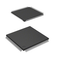
DF2166VTE33 Renesas Electronics America, DF2166VTE33 Datasheet - Page 393

DF2166VTE33
Manufacturer Part Number
DF2166VTE33
Description
MCU FLASH 3V 512K 33MHZ 144TQFP
Manufacturer
Renesas Electronics America
Series
H8® H8S/2100r
Datasheet
1.HS2168EPI61H-U.pdf
(876 pages)
Specifications of DF2166VTE33
Core Processor
H8S/2000
Core Size
16-Bit
Speed
33MHz
Connectivity
I²C, IrDA, LPC, SCI, SmartCard
Peripherals
POR, PWM, WDT
Number Of I /o
106
Program Memory Size
512KB (512K x 8)
Program Memory Type
FLASH
Ram Size
40K x 8
Voltage - Supply (vcc/vdd)
3 V ~ 3.6 V
Data Converters
A/D 8x10b; D/A 2x8b
Oscillator Type
External
Operating Temperature
-20°C ~ 75°C
Package / Case
144-TQFP, 144-VQFP
Lead Free Status / RoHS Status
Contains lead / RoHS non-compliant
Eeprom Size
-
- Current page: 393 of 876
- Download datasheet (5Mb)
This LSI has three independent serial communication interface (SCI) channels. The SCI can
handle both asynchronous and clock synchronous serial communication. Asynchronous serial data
communication can be carried out with standard asynchronous communication chips such as a
Universal Asynchronous Receiver/Transmitter (UART) or Asynchronous Communication
Interface Adapter (ACIA). A function is also provided for serial communication between
processors (multiprocessor communication function). The SCI also supports the smart card (IC
card) interface based on ISO/IEC 7816-3 (Identification Card) as an enhanced asynchronous
communication function.
SCI_1 can handle communication using the waveform based on the Infrared Data Association
(IrDA) standard version 1.0. SCI_0 and SCI_2 provide high-speed communication at an average
transfer rate of a specific system clock frequency. Reliable fast data transfers are secured using the
internal cyclic redundancy check (CRC) operation circuit. Since the CRC operation circuit is not
connected to the SCI, data is transferred to the circuit using the MOV instruction to be operated
there.
14.1
• Choice of asynchronous or clock synchronous serial communication mode
• Full-duplex communication capability
• On-chip baud rate generator allows any bit rate to be selected
• Choice of LSB-first or MSB-first transfer (except in the case of asynchronous mode 7-bit data)
• Four interrupt sources
• Module stop mode availability
SCI0022A_000120020900
The transmitter and receiver are mutually independent, enabling transmission and reception to
be executed simultaneously. Double-buffering is used in both the transmitter and the receiver,
enabling continuous transmission and continuous reception of serial data.
The external clock can be selected as a transfer clock source (except for the smart card
interface).
Four interrupt sources transmit-end, transmit-data-empty, receive-data-full, and receive
error that can issue requests.
The transmit-data-empty and receive-data-full interrupt sources can activate DTC.
Features
Section 14 Serial Communication Interface
(SCI, IrDA, and CRC)
Rev. 3.00, 03/04, page 351 of 830
Related parts for DF2166VTE33
Image
Part Number
Description
Manufacturer
Datasheet
Request
R

Part Number:
Description:
0.6mm Pitch Board-to-Fine-Coaxial Cable Connectors
Manufacturer:
Hirose Electric
Datasheet:

Part Number:
Description:
0.6mm Pitch Board-to-fine-coaxial Cable Connectors
Manufacturer:
Hirose Electric
Datasheet:

Part Number:
Description:
0.6mm Pitch Board-to-fine-coaxial Cable Connectors
Manufacturer:
Hirose Electric
Datasheet:

Part Number:
Description:
Right angle, Two-piece for fine coaxial cable, Discrete wire connectors; HRS No: 687-0001-5 56; No. of Positions: 20; Connector Type: Board mounting; Contact Gender: Female; Contact Spacing (mm): 0.6; Terminal Pitch (mm): 0.6; PCB Mount Type: SMT; Cu
Manufacturer:
Hirose Electric

Part Number:
Description:
0.6mm Pitch Board-to-fine-coaxial Cable Connectors
Manufacturer:
Hirose Electric
Datasheet:

Part Number:
Description:
0.6mm Pitch Board-to-Fine-Coaxial Cable Connectors
Manufacturer:
HIROSE [Hirose Electric]
Datasheet:

Part Number:
Description:
KIT STARTER FOR M16C/29
Manufacturer:
Renesas Electronics America
Datasheet:

Part Number:
Description:
KIT STARTER FOR R8C/2D
Manufacturer:
Renesas Electronics America
Datasheet:

Part Number:
Description:
R0K33062P STARTER KIT
Manufacturer:
Renesas Electronics America
Datasheet:

Part Number:
Description:
KIT STARTER FOR R8C/23 E8A
Manufacturer:
Renesas Electronics America
Datasheet:

Part Number:
Description:
KIT STARTER FOR R8C/25
Manufacturer:
Renesas Electronics America
Datasheet:

Part Number:
Description:
KIT STARTER H8S2456 SHARPE DSPLY
Manufacturer:
Renesas Electronics America
Datasheet:

Part Number:
Description:
KIT STARTER FOR R8C38C
Manufacturer:
Renesas Electronics America
Datasheet:

Part Number:
Description:
KIT STARTER FOR R8C35C
Manufacturer:
Renesas Electronics America
Datasheet:

Part Number:
Description:
KIT STARTER FOR R8CL3AC+LCD APPS
Manufacturer:
Renesas Electronics America
Datasheet:


