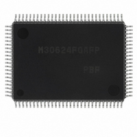
M30624FGAFP#U3 Renesas Electronics America, M30624FGAFP#U3 Datasheet - Page 441

M30624FGAFP#U3
Manufacturer Part Number
M30624FGAFP#U3
Description
IC M16C MCU FLASH 100QFP
Manufacturer
Renesas Electronics America
Series
M16C™ M16C/60r
Datasheets
1.M30622SAFPU5.pdf
(277 pages)
2.M30622SAFPU5.pdf
(617 pages)
3.M30622SAFPU5.pdf
(308 pages)
Specifications of M30624FGAFP#U3
Core Processor
M16C/60
Core Size
16-Bit
Speed
16MHz
Connectivity
SIO, UART/USART
Peripherals
DMA, PWM, WDT
Number Of I /o
85
Program Memory Size
256KB (256K x 8)
Program Memory Type
FLASH
Ram Size
20K x 8
Voltage - Supply (vcc/vdd)
4.2 V ~ 5.5 V
Data Converters
A/D 10x10b, D/A 2x8b
Oscillator Type
Internal
Operating Temperature
-40°C ~ 85°C
Package / Case
100-QFP
For Use With
867-1000 - KIT QUICK START RENESAS 62PM3062PT3-CPE-3 - EMULATOR COMPACT M16C/62P/30P
Lead Free Status / RoHS Status
Lead free / RoHS Compliant
Eeprom Size
-
Available stocks
Company
Part Number
Manufacturer
Quantity
Price
Part Number:
M30624FGAFP#U3M30624FGAFP#D3
Manufacturer:
Renesas Electronics America
Quantity:
10 000
Part Number:
M30624FGAFP#U3M30624FGAFP#D5
Manufacturer:
Renesas Electronics America
Quantity:
10 000
- Current page: 441 of 617
- Download datasheet (9Mb)
2-122
A-D Converter
Operation (1) Setting the A-D conversion start flag to “1” causes voltage input to the ANi pin to be output
Figure 2.7.11. Operation timing of one-shot mode, with external op-amp connection mode selected
2.7.5 Operation of A-D Converter (in one-shot mode, external op-amp connection mode selected)
In one-shot mode, choose functions from those listed in Table 2.7.5. Operations of the circled items are
described below. Figure 2.7.11 shows timing chart, and Figure 2.7.12 shows the set-up procedure.
Example of wiring
Input voltage
Input voltage
Op-amp
Table 2.7.5. Choosed functions
(2) After the A-D conversion is completed, the content of the successive comparison register
Analog input pin
Operation clock
Resolution
Trigger for starting
A-D conversion
AD
from the ANEX0 pin. The A-D conversion is carried out on voltage input to the ANEX1 pin
(connect an operation amplifier between the ANEX0 pin and the ANEX1 pin).
(conversion result) is transmitted to A-D register i corresponding to the ANi pin. At this time,
the A-D conversion interrupt request bit goes to “1”.
Item
AN
AN
ANEX0
ANEX1
Microcomputer
1
0
O
O
O
O
Divided-by-4 f
by-2 f
Software trigger
Trigger by AD
8-bit / 10-bit
One of AN
A-D conversion
start flag
A-D register i
A-D conversion
interrupt request
Example of operation
AD
Note: When
AD
/ f
Conversion rate per analog input pin is 49
10-bit resolution.
Set-up
AD
0
pin to AN
AD
TRG
AD
/ divided-
frequency is less than 1MH
“1”
“0”
“1”
“0”
7
pin
Cleared to “0” when interrupt request is accepted, or cleared by software
(1) Start A-D conversion
Set to “1” by software
8-bit resolution : 28
10-bit resolution : 33
Sample & Hold
Expanded analog
input pin
Z
, sample and hold function cannot be selected.
AD
Item
cycles for 8-bit resolution and 59
AD
SINGLE-CHIP 16-BIT CMOS MICROCOMPUTER
AD
cycles
cycles
(2) A-D conversion is complete
O
O
Not used
Either ANEX0 pin or
ANEX1 pin
External operation amplifier
connection mode
Not activated
Activated
Result
M16C / 62A Group
AD
Mitsubishi microcomputers
cycles for
Set-up
Related parts for M30624FGAFP#U3
Image
Part Number
Description
Manufacturer
Datasheet
Request
R

Part Number:
Description:
KIT STARTER FOR M16C/29
Manufacturer:
Renesas Electronics America
Datasheet:

Part Number:
Description:
KIT STARTER FOR R8C/2D
Manufacturer:
Renesas Electronics America
Datasheet:

Part Number:
Description:
R0K33062P STARTER KIT
Manufacturer:
Renesas Electronics America
Datasheet:

Part Number:
Description:
KIT STARTER FOR R8C/23 E8A
Manufacturer:
Renesas Electronics America
Datasheet:

Part Number:
Description:
KIT STARTER FOR R8C/25
Manufacturer:
Renesas Electronics America
Datasheet:

Part Number:
Description:
KIT STARTER H8S2456 SHARPE DSPLY
Manufacturer:
Renesas Electronics America
Datasheet:

Part Number:
Description:
KIT STARTER FOR R8C38C
Manufacturer:
Renesas Electronics America
Datasheet:

Part Number:
Description:
KIT STARTER FOR R8C35C
Manufacturer:
Renesas Electronics America
Datasheet:

Part Number:
Description:
KIT STARTER FOR R8CL3AC+LCD APPS
Manufacturer:
Renesas Electronics America
Datasheet:

Part Number:
Description:
KIT STARTER FOR RX610
Manufacturer:
Renesas Electronics America
Datasheet:

Part Number:
Description:
KIT STARTER FOR R32C/118
Manufacturer:
Renesas Electronics America
Datasheet:

Part Number:
Description:
KIT DEV RSK-R8C/26-29
Manufacturer:
Renesas Electronics America
Datasheet:

Part Number:
Description:
KIT STARTER FOR SH7124
Manufacturer:
Renesas Electronics America
Datasheet:

Part Number:
Description:
KIT STARTER FOR H8SX/1622
Manufacturer:
Renesas Electronics America
Datasheet:

Part Number:
Description:
KIT DEV FOR SH7203
Manufacturer:
Renesas Electronics America
Datasheet:


