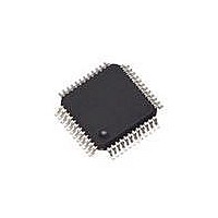
SAF-XC886CLM-8FFI 5V AC Infineon Technologies, SAF-XC886CLM-8FFI 5V AC Datasheet - Page 123

SAF-XC886CLM-8FFI 5V AC
Manufacturer Part Number
SAF-XC886CLM-8FFI 5V AC
Description
IC MCU 8BIT FLASH TQFP-48
Manufacturer
Infineon Technologies
Series
XC8xxr
Datasheet
1.SAF-XC888CLM-6FFA_5V_AC.pdf
(144 pages)
Specifications of SAF-XC886CLM-8FFI 5V AC
Program Memory Type
FLASH
Program Memory Size
32KB (32K x 8)
Package / Case
48-TFQFP
Core Processor
XC800
Core Size
8-Bit
Speed
103.2MHz
Connectivity
CAN, LIN, SSI, UART/USART
Peripherals
Brown-out Detect/Reset, POR, PWM, WDT
Number Of I /o
34
Ram Size
1.75K x 8
Voltage - Supply (vcc/vdd)
4.5 V ~ 5.5 V
Data Converters
A/D 8x10b
Oscillator Type
Internal
Operating Temperature
-40°C ~ 85°C
Data Bus Width
8 bit
Data Ram Size
1.75 KB
Interface Type
JTAG/SPI/SSC/UART
Maximum Clock Frequency
24 MHz
Number Of Programmable I/os
48
Number Of Timers
4
Operating Supply Voltage
5 V
Maximum Operating Temperature
+ 85 C
Mounting Style
SMD/SMT
Minimum Operating Temperature
- 40 C
On-chip Adc
8-ch x 10-bit
Lead Free Status / RoHS Status
Contains lead / RoHS non-compliant
For Use With
MCBXC88X - BOARD EVAL FOR INFINEON XC88X
Eeprom Size
-
Lead Free Status / Rohs Status
Lead free / RoHS Compliant
Other names
FX886CLM8FFI5VACXT
SAF-XC886CLM-8FFI AB
SAF-XC886CLM-8FFI AB
SAFXC886CLM8FFIABT
SP000217341
SAF-XC886CLM-8FFI AB
SAF-XC886CLM-8FFI AB
SAFXC886CLM8FFIABT
SP000217341
4.2.3
The values in the table below are given for an analog power supply between 4.5 V to
5.5 V. The ADC can be used with an analog power supply down to 3 V. But in this case,
the analog parameters may show a reduced performance. All ground pins (
externally connected to one single star point in the system. The voltage difference
between the ground pins must not exceed 200mV.
Table 40
Parameter
Analog reference
voltage
Analog reference
ground
Analog input
voltage range
ADC clocks
Sample time
Conversion time
Total unadjusted
error
Differential
Nonlinearity
Integral
Nonlinearity
Offset
Gain
Overload current
coupling factor for
analog inputs
Data Sheet
ADC Characteristics
ADC Characteristics (Operating Conditions apply;
Symbol
V
V
V
f
f
t
t
|TUE|
|
|
|
|
K
EA
EA
EA
EA
ADC
ADCI
S
C
AREF
AGND
AIN
OVA
DNL
INL
OFF
GAIN
|
|
|
| CC –
SR
SR
SR
CC (2 + INPCR0.STC) ×
CC See
CC –
CC –
CC –
CC –
CC –
min.
V
+ 1
V
0.05
V
–
–
–
–
t
ADCI
AGND
SS
AGND
Limit Values
-
Section 4.2.3.1
116
typ .
V
V
–
24
–
–
–
1
1
1
1
–
–
DDP
SS
max.
V
+ 0.05
V
- 1
V
25.8
10
1
2
–
–
–
–
1.0 x
10
1.5 x
10
DDP
AREF
AREF
-4
-3
Unit Test Conditions/
V
V
V
MHz module clock
MHz internal analog clock
µs
µs
LSB 8-bit conversion
LSB 10-bit conversion
LSB 10-bit conversion
LSB 10-bit conversion
LSB 10-bit conversion
LSB 10-bit conversion
–
–
Electrical Parameters
Remarks
1)
1)
See
1)
1)
I
I
OV
OV
V
> 0
< 0
XC886/888CLM
Figure 35
DDP
1)3)
1)3)
= 5V Range)
V
V1.2, 2009-07
SS
) must be
1)
2)
2)
1)
1)
1)
1)
1)


