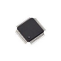
SAF-XC886CLM-8FFI 5V AC Infineon Technologies, SAF-XC886CLM-8FFI 5V AC Datasheet - Page 61

SAF-XC886CLM-8FFI 5V AC
Manufacturer Part Number
SAF-XC886CLM-8FFI 5V AC
Description
IC MCU 8BIT FLASH TQFP-48
Manufacturer
Infineon Technologies
Series
XC8xxr
Datasheet
1.SAF-XC888CLM-6FFA_5V_AC.pdf
(144 pages)
Specifications of SAF-XC886CLM-8FFI 5V AC
Program Memory Type
FLASH
Program Memory Size
32KB (32K x 8)
Package / Case
48-TFQFP
Core Processor
XC800
Core Size
8-Bit
Speed
103.2MHz
Connectivity
CAN, LIN, SSI, UART/USART
Peripherals
Brown-out Detect/Reset, POR, PWM, WDT
Number Of I /o
34
Ram Size
1.75K x 8
Voltage - Supply (vcc/vdd)
4.5 V ~ 5.5 V
Data Converters
A/D 8x10b
Oscillator Type
Internal
Operating Temperature
-40°C ~ 85°C
Data Bus Width
8 bit
Data Ram Size
1.75 KB
Interface Type
JTAG/SPI/SSC/UART
Maximum Clock Frequency
24 MHz
Number Of Programmable I/os
48
Number Of Timers
4
Operating Supply Voltage
5 V
Maximum Operating Temperature
+ 85 C
Mounting Style
SMD/SMT
Minimum Operating Temperature
- 40 C
On-chip Adc
8-ch x 10-bit
Lead Free Status / RoHS Status
Contains lead / RoHS non-compliant
For Use With
MCBXC88X - BOARD EVAL FOR INFINEON XC88X
Eeprom Size
-
Lead Free Status / Rohs Status
Lead free / RoHS Compliant
Other names
FX886CLM8FFI5VACXT
SAF-XC886CLM-8FFI AB
SAF-XC886CLM-8FFI AB
SAFXC886CLM8FFIABT
SP000217341
SAF-XC886CLM-8FFI AB
SAF-XC886CLM-8FFI AB
SAFXC886CLM8FFIABT
SP000217341
Figure 11
The internal structure of each Flash bank represents a sector architecture for flexible
erase capability. The minimum erase width is always a complete sector, and sectors can
be erased separately or in parallel. Contrary to standard EPROMs, erased Flash
memory cells contain 0s.
The D-Flash bank is divided into more physical sectors for extended erasing and
reprogramming capability; even numbers for each sector size are provided to allow
greater flexibility and the ability to adapt to a wide range of application requirements.
3.3.2
To enhance system performance, the P-Flash banks are configured for parallel read to
allow two bytes of linear code to be read in 4 x CCLK cycles, compared to 6 x CCLK
cycles if serial read is performed. This is achieved by reading two bytes in parallel from
a P-Flash bank pair within the 3 x CCLK cycles access time and storing them in a cache.
Subsequent read from the cache by the CPU does not require a wait state and can be
completed within 1 x CCLK cycle. The result is the average instruction fetch time from
the P-Flash banks is reduced and thus, the MIPS (Mega Instruction Per Second) of the
system is increased.
However, if the parallel read feature is not desired due to certain timing constraints, it can
be disabled by calling the parallel read disable subroutine.
Data Sheet
Parallel Read Access of P-Flash
Sector 0: 3.75-Kbyte
Flash Bank Sectorization
Sector 2: 128-byte
Sector 1: 128-byte
P-Flash
54
Sector 3: 512-byte
Sector 9: 128-byte
Sector 8: 128-byte
Sector 7: 128-byte
Sector 6: 128-byte
Sector 5: 256-byte
Sector 4: 256-byte
Sector 2: 512-byte
Sector 1: 1-Kbyte
Sector 0: 1-Kbyte
D-Flash
Functional Description
XC886/888CLM
V1.2, 2009-07


