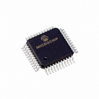
PIC16LC774/PQ Microchip Technology, PIC16LC774/PQ Datasheet - Page 27

PIC16LC774/PQ
Manufacturer Part Number
PIC16LC774/PQ
Description
IC MCU OTP 4KX14 A/D PWM 44-MQFP
Manufacturer
Microchip Technology
Series
PIC® 16Cr
Specifications of PIC16LC774/PQ
Core Processor
PIC
Core Size
8-Bit
Speed
20MHz
Connectivity
I²C, SPI, UART/USART
Peripherals
Brown-out Detect/Reset, POR, PWM, WDT
Number Of I /o
33
Program Memory Size
7KB (4K x 14)
Program Memory Type
OTP
Ram Size
256 x 8
Voltage - Supply (vcc/vdd)
2.5 V ~ 5.5 V
Data Converters
A/D 10x12b
Oscillator Type
External
Operating Temperature
0°C ~ 70°C
Package / Case
44-MQFP, 44-PQFP
Processor Series
PIC16LC
Core
PIC
Data Bus Width
8 bit
Data Ram Size
256 B
Interface Type
I2C, SPI, SSP, UART
Maximum Clock Frequency
20 MHz
Number Of Programmable I/os
33
Number Of Timers
3 bit
Operating Supply Voltage
2.5 V to 5.5 V
Maximum Operating Temperature
+ 70 C
Mounting Style
SMD/SMT
3rd Party Development Tools
52715-96, 52716-328, 52717-734
Development Tools By Supplier
ICE2000, DM163022
Minimum Operating Temperature
0 C
On-chip Adc
10 bit
Lead Free Status / RoHS Status
Lead free / RoHS Compliant
Eeprom Size
-
Lead Free Status / Rohs Status
Details
Available stocks
Company
Part Number
Manufacturer
Quantity
Price
Company:
Part Number:
PIC16LC774/PQ
Manufacturer:
Microchip Technology
Quantity:
10 000
3.0
Some pins for these I/O ports are multiplexed with an
alternate function for the peripheral features on the
device. In general, when a peripheral is enabled, that
pin may not be used as a general purpose I/O pin.
Additional information on I/O ports may be found in the
PICmicro™
(DS33023).
3.1
PORTA is a 6-bit wide bi-directional port for the 40/44
pin devices and is 5-bits wide for the 28-pin devices.
PORTA<5> is not on the 28-pin devices. The corre-
sponding data direction register is TRISA. Setting a
TRISA bit (=1) will make the corresponding PORTA pin
an input, i.e., put the corresponding output driver in a
hi-impedance mode. Clearing a TRISA bit (=0) will
make the corresponding PORTA pin an output, i.e., put
the contents of the output latch on the selected pin.
Reading the PORTA register reads the status of the
pins whereas writing to it will write to the port latch. All
write operations are read-modify-write operations.
Therefore a write to a port implies that the port pins are
read, this value is modified, and then written to the port
data latch.
Pin RA4 is multiplexed with the Timer0 module clock
input to become the RA4/T0CKI pin. The RA4/T0CKI
pin is a Schmitt Trigger input and an open drain output.
All other RA port pins have TTL input levels and full
CMOS output drivers.
Other PORTA pins are multiplexed with analog inputs
and analog V
ences (VRL/VRH). The operation of each pin is
selected by clearing/setting the control bits in the
ADCON1 register (A/D Control Register1).
The TRISA register controls the direction of the RA
pins, even when they are being used as analog inputs.
The user must ensure the bits in the TRISA register are
maintained set when using them as analog inputs.
EXAMPLE 3-1:
BCF
CLRF
BSF
MOVLW
MOVWF
Note:
1999 Microchip Technology Inc.
STATUS, RP0
PORTA
STATUS, RP0
0xCF
TRISA
I/O PORTS
PORTA and the TRISA Register
On a Power-on Reset, these pins are con-
figured as analog inputs and read as '0'.
REF
Mid-Range
inputs and precision on-board refer-
INITIALIZING PORTA
;
; Initialize PORTA by
; clearing output
; data latches
; Select Bank 1
; Value used to
; initialize data
; direction
; Set RA<3:0> as inputs
; RA<5:4> as outputs
; TRISA<7:6> are always
; read as ’0’.
Reference
Advance Information
Manual,
FIGURE 3-1:
VRHOEN, VRLOEN
Sense input for
VRH, VRL
VRO+, VRO- amplifier
Data
bus
WR
Port
WR
TRIS
RD PORT
To A/D Converter
Note 1: I/O pins have protection diodes to V
V
D
Data Latch
D
TRIS Latch
SS
CK
CK
.
BLOCK DIAGRAM OF
RA3:RA2 PINS
Q
Q
Q
Q
RD TRIS
PIC16C77X
Q
Analog
input
mode
EN
DS30275A-page 27
D
V
V
P
N
SS
DD
DD
and
TTL
input
buffer
I/O pin
(1)


