PIC16LC774/PQ Microchip Technology, PIC16LC774/PQ Datasheet - Page 28
PIC16LC774/PQ
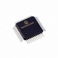
Manufacturer Part Number
PIC16LC774/PQ
Description
IC MCU OTP 4KX14 A/D PWM 44-MQFP
Manufacturer
Microchip Technology
Series
PIC® 16Cr
Specifications of PIC16LC774/PQ
Core Processor
PIC
Core Size
8-Bit
Speed
20MHz
Connectivity
I²C, SPI, UART/USART
Peripherals
Brown-out Detect/Reset, POR, PWM, WDT
Number Of I /o
33
Program Memory Size
7KB (4K x 14)
Program Memory Type
OTP
Ram Size
256 x 8
Voltage - Supply (vcc/vdd)
2.5 V ~ 5.5 V
Data Converters
A/D 10x12b
Oscillator Type
External
Operating Temperature
0°C ~ 70°C
Package / Case
44-MQFP, 44-PQFP
Processor Series
PIC16LC
Core
PIC
Data Bus Width
8 bit
Data Ram Size
256 B
Interface Type
I2C, SPI, SSP, UART
Maximum Clock Frequency
20 MHz
Number Of Programmable I/os
33
Number Of Timers
3 bit
Operating Supply Voltage
2.5 V to 5.5 V
Maximum Operating Temperature
+ 70 C
Mounting Style
SMD/SMT
3rd Party Development Tools
52715-96, 52716-328, 52717-734
Development Tools By Supplier
ICE2000, DM163022
Minimum Operating Temperature
0 C
On-chip Adc
10 bit
Lead Free Status / RoHS Status
Lead free / RoHS Compliant
Eeprom Size
-
Lead Free Status / Rohs Status
Details
Available stocks
Company
Part Number
Manufacturer
Quantity
Price
Company:

Part Number:
PIC16LC774/PQ
Manufacturer:
Microchip Technology
Quantity:
10 000


PIC16C77X
FIGURE 3-2:
TABLE 3-1
TABLE 3-2
DS30275A-page 28
Name
RA0/AN0
RA1/AN1
RA2/AN2/V
RA3/AN3/V
RA4/T0CKI
RA5/AN4
Legend: TTL = TTL input, ST = Schmitt Trigger input
Note 1: RA5 is reserved on the 28-pin devices, maintain this bit clear.
Address
05h
85h
9Fh
Legend: x = unknown, u = unchanged, - = unimplemented locations read as '0'. Shaded cells are not used by PORTA.
Note 1:
Data
bus
WR
Port
WR
TRIS
RD PORT
To A/D Converter
Note 1: I/O pins have protection diodes to V
PORTA<5>, TRISA<5> are reserved on the 28-pin devices, maintain these bits clear.
(1)
Name
PORTA
TRISA
ADCON1
V
D
D
Data Latch
TRIS Latch
SS
REF
REF
CK
CK
.
-/VRL
+/VRH
(1)
(1)
BLOCK DIAGRAM OF
RA1:RA0 AND RA5 PINS
PORTA FUNCTIONS
SUMMARY OF REGISTERS ASSOCIATED WITH PORTA
Q
Q
Q
Q
RD TRIS
ADFM VCFG2
Bit 7
—
—
Bit#
bit0
bit1
bit2
bit3
bit4
bit5
Q
Bit 6
—
—
Analog
input
mode
EN
D
Buffer
TTL
TTL
TTL
TTL
ST
TTL
PORTA Data Direction Register
VCFG1 VCFG0
V
V
P
N
Bit 5
RA5
SS
DD
DD
Advance Information
and
I/O pin
TTL
input
buffer
Function
Input/output or analog input0
Input/output or analog input1
Input/output or analog input2 or V
voltage low
Input/output or analog input or V
reference voltage high
Input/output or external clock input for Timer0
Output is open drain type
Input/output or analog input
Bit 4
RA4
(1)
PCFG3
Bit 3
RA3
FIGURE 3-3:
PCFG2
Bit 2
RA2
Data
bus
WR
TRIS
WR
PORT
RD PORT
Note 1: I/O pin has protection diodes to V
TMR0 clock input
PCFG1
Bit 1
RA1
TRIS Latch
Data Latch
REF
D
D
CK
CK
REF
RD TRIS
BLOCK DIAGRAM OF
RA4/T0CKI PIN
+ input or output of internal
PCFG0
- input or internal reference
Bit 0
RA0
Q
Q
Q
Q
1999 Microchip Technology Inc.
--0x 0000
--11 1111
0000 0000
Value on:
Q
POR,
BOR
EN
Schmitt
Trigger
input
buffer
EN
D
V
N
SS
other resets
Value on all
SS
--0u 0000
--11 1111
0000 0000
I/O pin
only.
(1)
Related parts for PIC16LC774/PQ
Image
Part Number
Description
Manufacturer
Datasheet
Request
R

Part Number:
Description:
3.5KB Flash, 128B RAM, 18 I/O, CLC, CWG, DDS, 10-bit ADC 20 QFN 4x4mm TUBE
Manufacturer:
Microchip Technology
Datasheet:

Part Number:
Description:
3.5KB Flash, 128B RAM, 18 I/O, CLC, CWG, DDS, 10-bit ADC 20 PDIP .300in TUBE
Manufacturer:
Microchip Technology
Datasheet:

Part Number:
Description:
3.5KB Flash, 128B RAM, 18 I/O, CLC, CWG, DDS, 10-bit ADC 20 SOIC .300in TUBE
Manufacturer:
Microchip Technology
Datasheet:

Part Number:
Description:
3.5KB Flash, 128B RAM, 18 I/O, CLC, CWG, DDS, 10-bit ADC 20 SSOP .209in TUBE
Manufacturer:
Microchip Technology
Datasheet:
Part Number:
Description:
3.5KB Flash, 128B RAM, 18 I/O, CLC, CWG, DDS, 10-bit ADC 20 QFN 4x4mm TUBE
Manufacturer:
Microchip Technology
Datasheet:
Part Number:
Description:
3.5KB Flash, 128B RAM, 18 I/O, CLC, CWG, DDS, 10-bit ADC 20 PDIP .300in TUBE
Manufacturer:
Microchip Technology
Datasheet:
Part Number:
Description:
3.5KB Flash, 128B RAM, 18 I/O, CLC, CWG, DDS, 10-bit ADC 20 SOIC .300in TUBE
Manufacturer:
Microchip Technology
Datasheet:
Part Number:
Description:
3.5KB Flash, 128B RAM, 18 I/O, CLC, CWG, DDS, 10-bit ADC 20 SSOP .209in TUBE
Manufacturer:
Microchip Technology
Datasheet:
Part Number:
Description:
3.5KB Flash, 128B RAM, 18 I/O, CLC, CWG, DDS, 10-bit ADC 20 QFN 4x4mm T/R
Manufacturer:
Microchip Technology
Datasheet:
Part Number:
Description:
3.5KB Flash, 128B RAM, 18 I/O, CLC, CWG, DDS, 10-bit ADC 20 SOIC .300in T/R
Manufacturer:
Microchip Technology
Datasheet:
Part Number:
Description:
3.5KB Flash, 128B RAM, 18 I/O, CLC, CWG, DDS, 10-bit ADC 20 SSOP .209in T/R
Manufacturer:
Microchip Technology
Datasheet:
Part Number:
Description:
3.5KB Flash, 128B RAM, 18 I/O, CLC, CWG, DDS, 10-bit ADC 20 QFN 4x4mm TUBE
Manufacturer:
Microchip Technology
Datasheet:
Part Number:
Description:
3.5KB Flash, 128B RAM, 18 I/O, CLC, CWG, DDS, 10-bit ADC 20 PDIP .300in TUBE
Manufacturer:
Microchip Technology
Datasheet:
Part Number:
Description:
3.5KB Flash, 128B RAM, 18 I/O, CLC, CWG, DDS, 10-bit ADC 20 SOIC .300in TUBE
Manufacturer:
Microchip Technology
Datasheet:
Part Number:
Description:
3.5KB Flash, 128B RAM, 18 I/O, CLC, CWG, DDS, 10-bit ADC 20 SSOP .209in TUBE
Manufacturer:
Microchip Technology
Datasheet: