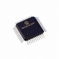
PIC16LC774/PQ Microchip Technology, PIC16LC774/PQ Datasheet - Page 65

PIC16LC774/PQ
Manufacturer Part Number
PIC16LC774/PQ
Description
IC MCU OTP 4KX14 A/D PWM 44-MQFP
Manufacturer
Microchip Technology
Series
PIC® 16Cr
Specifications of PIC16LC774/PQ
Core Processor
PIC
Core Size
8-Bit
Speed
20MHz
Connectivity
I²C, SPI, UART/USART
Peripherals
Brown-out Detect/Reset, POR, PWM, WDT
Number Of I /o
33
Program Memory Size
7KB (4K x 14)
Program Memory Type
OTP
Ram Size
256 x 8
Voltage - Supply (vcc/vdd)
2.5 V ~ 5.5 V
Data Converters
A/D 10x12b
Oscillator Type
External
Operating Temperature
0°C ~ 70°C
Package / Case
44-MQFP, 44-PQFP
Processor Series
PIC16LC
Core
PIC
Data Bus Width
8 bit
Data Ram Size
256 B
Interface Type
I2C, SPI, SSP, UART
Maximum Clock Frequency
20 MHz
Number Of Programmable I/os
33
Number Of Timers
3 bit
Operating Supply Voltage
2.5 V to 5.5 V
Maximum Operating Temperature
+ 70 C
Mounting Style
SMD/SMT
3rd Party Development Tools
52715-96, 52716-328, 52717-734
Development Tools By Supplier
ICE2000, DM163022
Minimum Operating Temperature
0 C
On-chip Adc
10 bit
Lead Free Status / RoHS Status
Lead free / RoHS Compliant
Eeprom Size
-
Lead Free Status / Rohs Status
Details
Available stocks
Company
Part Number
Manufacturer
Quantity
Price
Company:
Part Number:
PIC16LC774/PQ
Manufacturer:
Microchip Technology
Quantity:
10 000
8.2.1.2
When the R/W bit of the address byte is clear and an
address match occurs, the R/W bit of the SSPSTAT
register is cleared. The received address is loaded into
the SSPBUF register.
When the address byte overflow condition exists, then
no acknowledge (ACK) pulse is given. An overflow con-
dition is defined as either bit BF (SSPSTAT<0>) is set
or bit SSPOV (SSPCON<6>) is set.
TABLE 8-2
8.2.1.3
When the R/W bit of the incoming address byte is set
and an address match occurs, the R/W bit of the
SSPSTAT register is set. The received address is
loaded into the SSPBUF register. The ACK pulse will
be sent on the ninth bit, and the SCL pin is held low.
The transmit data must be loaded into the SSPBUF
register, which also loads the SSPSR register. Then the
SCL pin should be enabled by setting bit CKP (SSP-
CON<4>). The master must monitor the SCL pin prior
to asserting another clock pulse. The slave devices
may be holding off the master by stretching the clock.
The eight data bits are shifted out on the falling edge of
the SCL input. This ensures that the SDA signal is valid
during the SCL high time
FIGURE 8-12: I
Note 1:
SDA
SCL
SSPIF
BF (SSPSTAT<0>)
1999 Microchip Technology Inc.
SSPOV (SSPCON<6>)
Transfer is Received
Status Bits as Data
BF
0
1
1
0
S
Shaded cells show the conditions where the user software did not properly clear the overflow condition.
SLAVE RECEPTION
SLAVE TRANSMISSION
A7 A6 A5 A4 A3 A2 A1
1
SSPOV
2
Receiving Address
DATA TRANSFER RECEIVED BYTE ACTIONS
2
0
0
1
1
3
C WAVEFORMS FOR RECEPTION (7-BIT ADDRESS)
4
(Figure
5
6
SSPSR
8-13).
7
R/W=0
8
ACK
9
Yes
Yes
No
No
Advance Information
D7
SSPBUF
1
D6
2
SSPBUF register is read
Cleared in software
Receiving Data
D5
3
D4
Bit SSPOV is set because the SSPBUF register is still full.
4
D3
5
D2
6
An SSP interrupt is generated for each data transfer
byte. Flag bit SSPIF (PIR1<3>) must be cleared in soft-
ware. The SSPSTAT register is used to determine the
status of the received byte.
An SSP interrupt is generated for each data transfer
byte. The SSPIF flag bit must be cleared in software,
and the SSPSTAT register is used to determine the sta-
tus of the byte tranfer. The SSPIF flag bit is set on the
falling edge of the ninth clock pulse.
As a slave-transmitter, the ACK pulse from the master-
receiver is latched on the rising edge of the ninth SCL
input pulse. If the SDA line was high (not ACK), then the
data transfer is complete. When the not ACK is latched
by the slave, the slave logic is reset and the slave then
monitors for another occurrence of the START bit. If the
SDA line was low (ACK), the transmit data must be
loaded into the SSPBUF register, which also loads the
SSPSR register. Then the SCL pin should be enabled
by setting the CKP bit.
Generate ACK
D1
7
Note:
Pulse
D0
8
Yes
No
No
No
ACK
9
The SSPBUF will be loaded if the SSPOV
bit is set and the BF flag is cleared. If a
read of the SSPBUF was performed, but
the user did not clear the state of the
SSPOV bit before the next receive
occured. The ACK is not sent and the SSP-
BUF is updated.
D7
1
D6
2
D5
Receiving Data
3
D4
4
ACK is not sent.
PIC16C77X
(SSP Interrupt occurs
D3
5
D2
6
Set bit SSPIF
if enabled)
D1
7
Yes
Yes
Yes
Yes
DS30275A-page 65
D0
8
ACK
Not
9
transfer
Bus Master
terminates
P


