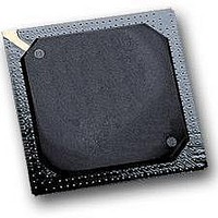
MPC5553MZQ132 Freescale Semiconductor, MPC5553MZQ132 Datasheet - Page 16

MPC5553MZQ132
Manufacturer Part Number
MPC5553MZQ132
Description
IC MCU MPC5553 REV A 324-PBGA
Manufacturer
Freescale Semiconductor
Series
MPC55xx Qorivvar
Datasheet
1.MPC5553EVBE.pdf
(68 pages)
Specifications of MPC5553MZQ132
Core Processor
e200z6
Core Size
32-Bit
Speed
132MHz
Connectivity
CAN, EBI/EMI, Ethernet, SCI, SPI
Peripherals
DMA, POR, PWM, WDT
Number Of I /o
220
Program Memory Size
1.5MB (1.5M x 8)
Program Memory Type
FLASH
Ram Size
64K x 8
Voltage - Supply (vcc/vdd)
1.35 V ~ 1.65 V
Data Converters
A/D 40x12b
Oscillator Type
External
Operating Temperature
-40°C ~ 125°C
Package / Case
324-PBGA
Processor Series
MPC5xxx
Core
e200z6
Data Bus Width
32 bit
Data Ram Size
64 KB
Interface Type
7-Wire, DSPI, ESCI
Maximum Clock Frequency
132 MHz
Number Of Timers
56
Maximum Operating Temperature
+ 125 C
Mounting Style
SMD/SMT
Minimum Operating Temperature
- 40 C
For Use With
MPC5553EVBISYS - KIT EVAL ISYSTEMS MPC5553MPC5553EVBGHS - KIT EVAL GREEN HILLS SOFTWAREMPC5553EVB - KIT EVAL MPC5553MZP132MPC5553EVBE - BOARD EVAL FOR MPC5553
Lead Free Status / RoHS Status
Lead free / RoHS Compliant
Eeprom Size
-
Lead Free Status / Rohs Status
No
Available stocks
Company
Part Number
Manufacturer
Quantity
Price
Company:
Part Number:
MPC5553MZQ132
Manufacturer:
Freescale Semiconductor
Quantity:
10 000
1
2
3
4
5
6
7
8
9
10
11
12
13
14
Spec
35a Analog input current, shared analog / digital pins
43a V
32
33
34
35
36
37
38
39
40
41
42
43
44
45
46
V
| V
V
If standby operation is not required, connect V
Applies to CLKOUT, external bus pins, and Nexus pins.
Maximum average RMS DC current.
Figure 3
Average current measured on Automotive benchmark.
Peak currents can be higher on specialized code.
High use current measured while running optimized SPE assembly code with all code and data 100% locked in cache
(0% miss rate) with all channels of the eMIOS and eTPU running autonomously, plus the eDMA transferring data continuously from
SRAM to SRAM. Higher currents are possible if an idle loop that crosses cache lines is run from cache. Design and write code to
avoid this condition.
Figure 3
Power requirements for the V
segments. Refer to
Power requirements for each I/O segment are dependent on the frequency of operation and load of the I/O pins on a particular I/O
segment, and the voltage of the I/O segment. Refer to
total power consumption of an I/O segment is the sum of the individual power consumptions for each pin on the segment.
Absolute value of current, measured at V
Electrical Characteristics
16
DDE2
PP
DDA0
can drop to 3.0 V during read operations.
Slow and medium I/O weak pullup/down current
I/O input leakage current
DC injection current (per pin)
Analog input current, channel off
(AN[12], AN[13], AN[14], AN[15])
V
Analog reference low voltage
V
Analog reference high voltage
V
V
V
V
Analog input differential signal range (with common mode 2.5 V)
Operating temperature range, ambient (packaged)
Slew rate on power-supply pins
SS
RL
REF
SSSYN
RCVSS
DDF
RC33
and V
3.0–3.6 V
4.5–5.5 V
– V
shows an illustration of the I
shows an illustration of the I
differential voltage
to V
differential voltage
to V
to V
DDA1
to V
DDE3
to V
SSA
DD
DDSYN
| must be < 0.1 V.
SS
SS
differential voltage
differential voltage
are limited to 2.25–3.6 V only if EBTS = 0; V
Table 11
differential voltage
differential voltage
differential voltage
Table 9. DC Electrical Specifications (T
for values to calculate the power dissipation for a specific operation.
DD33
15
Characteristic
supply depend on the frequency of operation, load of all I/O pins, and the voltages on the I/O
17
DD_STBY
DD_STBY
16
MPC5553 Microcontroller Data Sheet, Rev. 3.0
IL
and V
values interpolated for these temperature values.
values interpolated for these temperature values.
STBY
IH
.
to ground.
14
Table 10
DDE2
for values to calculate power dissipation for specific operation. The
and V
V
A
T
V
V
DDE3
RC33
A
V
V
V
= T
SSSYN
RCVSS
V
I
DDF
SS
= (T
I
INACT_AD
RL
Symbol
I
RH
INACT_D
INACT_A
I
V
ACT_S
V
V
L
have a range of 1.6–3.6 V if EBTS = 1.
– V
IDIFF
– V
I
– V
—
IC
RH
RL
– V
L
– T
– V
– V
– V
to T
DDSYN
SSA
SSA
RL
DD
H
SS
SS
) (continued)
H
)
V
V
SSA
DDA
–150
–100
–100
–100
–2.5
–2.0
–2.5
–0.1
–2.5
Min
–50
–50
4.5
10
20
T
—
L
– 0.1
– 0.1
Freescale Semiconductor
V
V
DDA
SSA
0.1
Max.
5.25
150
170
150
100
100
100
2.5
2.0
2.5
2.5
T
50
50
50
H
+ 0.1
+ 0.1
18
V/ms
Unit
mA
mV
mV
mV
mV
mV
μA
μA
μA
nA
μA
ο
V
V
V
V
V
C


