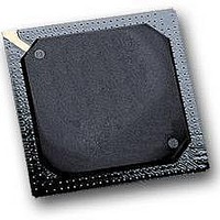
MPC5553MZQ132 Freescale Semiconductor, MPC5553MZQ132 Datasheet - Page 61

MPC5553MZQ132
Manufacturer Part Number
MPC5553MZQ132
Description
IC MCU MPC5553 REV A 324-PBGA
Manufacturer
Freescale Semiconductor
Series
MPC55xx Qorivvar
Datasheet
1.MPC5553EVBE.pdf
(68 pages)
Specifications of MPC5553MZQ132
Core Processor
e200z6
Core Size
32-Bit
Speed
132MHz
Connectivity
CAN, EBI/EMI, Ethernet, SCI, SPI
Peripherals
DMA, POR, PWM, WDT
Number Of I /o
220
Program Memory Size
1.5MB (1.5M x 8)
Program Memory Type
FLASH
Ram Size
64K x 8
Voltage - Supply (vcc/vdd)
1.35 V ~ 1.65 V
Data Converters
A/D 40x12b
Oscillator Type
External
Operating Temperature
-40°C ~ 125°C
Package / Case
324-PBGA
Processor Series
MPC5xxx
Core
e200z6
Data Bus Width
32 bit
Data Ram Size
64 KB
Interface Type
7-Wire, DSPI, ESCI
Maximum Clock Frequency
132 MHz
Number Of Timers
56
Maximum Operating Temperature
+ 125 C
Mounting Style
SMD/SMT
Minimum Operating Temperature
- 40 C
For Use With
MPC5553EVBISYS - KIT EVAL ISYSTEMS MPC5553MPC5553EVBGHS - KIT EVAL GREEN HILLS SOFTWAREMPC5553EVB - KIT EVAL MPC5553MZP132MPC5553EVBE - BOARD EVAL FOR MPC5553
Lead Free Status / RoHS Status
Lead free / RoHS Compliant
Eeprom Size
-
Lead Free Status / Rohs Status
No
Available stocks
Company
Part Number
Manufacturer
Quantity
Price
Company:
Part Number:
MPC5553MZQ132
Manufacturer:
Freescale Semiconductor
Quantity:
10 000
Freescale Semiconductor
Section 3.7.1, “Input Value of Pins During POR Dependent on
Location
From:
Added the following text directly before this section and after
Power-on Sequence:
To:
‘When powering the device, V
‘To avoid accidentally selecting the bypass clock because PLLCFG[0:1] and RSTCFG are not treated as ones
V
internal versions of PLLCFG[0:1] and RSTCFG are not powered and therefore cannot read the default state
when POR negates. V
the V
requirements when powering down.’
‘The values in
power up.
Before exiting the internal POR state, the voltage on the pins goes to high-impedance until POR negates. When
the internal POR negates, the functional state of the signal during reset applies and the weak pull devices (up or
down) are enabled as defined in the device Reference Manual. If V
signals, the weak-pull devices can pull the signals to V
To avoid this condition, minimize the ramp time of the V
enable the external circuitry connected to the device outputs.’
(1s) when POR negates, V
device by more than the V
RESET power pin (V
V
applies during power up. V
DD33
DDEH6
Table 32. Global and Text Changes Between Rev. 2.0 and 3.0 (continued)
DD33
lag specification listed in
supplies, but cannot lag both by more than the V
lag specification. This V
Table 7
DDEH6
DD33
and
MPC5553 Microcontroller Data Sheet, Rev. 3.0
DD33
Table 8
DD33
DD33
) by more than the V
can lag V
DD33
lag specification in
Table
has no lead or lag requirements when powering down.’
must not lag V
DD33
do not include the effect of the weak pull devices on the output pins during
must not lag V
DDSYN
6. This avoids accidentally selecting the bypass clock mode because the
lag specification only applies during power up. V
Description of Change
or the RESET power pin (V
DDSYN
VDD33,” changed:
DD33
DDSYN
Table
lag specification. V
and the RESET pin power (V
DDE
DD
DD33
and the RESET power pin (V
6. V
Table 8
supply to a time period less than the time required to
and V
DD33
lag specification. This V
Revision History for the MPC5553 Data Sheet
DDEH
Pin Status for Medium / Slow Pads During the
individually can lag either V
DD
is too low to correctly propagate the logic
DDEH6
.
DD33
), but cannot lag both by more than
can lag one of the V
DDEH6
DD33
DDEH6
DD33
) when powering the
lag specification only
) by more than the
has no lead or lag
DDSYN
DDSYN
or the
or
61


