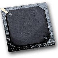
MPC5553MZQ132 Freescale Semiconductor, MPC5553MZQ132 Datasheet - Page 22

MPC5553MZQ132
Manufacturer Part Number
MPC5553MZQ132
Description
IC MCU MPC5553 REV A 324-PBGA
Manufacturer
Freescale Semiconductor
Series
MPC55xx Qorivvar
Datasheet
1.MPC5553EVBE.pdf
(68 pages)
Specifications of MPC5553MZQ132
Core Processor
e200z6
Core Size
32-Bit
Speed
132MHz
Connectivity
CAN, EBI/EMI, Ethernet, SCI, SPI
Peripherals
DMA, POR, PWM, WDT
Number Of I /o
220
Program Memory Size
1.5MB (1.5M x 8)
Program Memory Type
FLASH
Ram Size
64K x 8
Voltage - Supply (vcc/vdd)
1.35 V ~ 1.65 V
Data Converters
A/D 40x12b
Oscillator Type
External
Operating Temperature
-40°C ~ 125°C
Package / Case
324-PBGA
Processor Series
MPC5xxx
Core
e200z6
Data Bus Width
32 bit
Data Ram Size
64 KB
Interface Type
7-Wire, DSPI, ESCI
Maximum Clock Frequency
132 MHz
Number Of Timers
56
Maximum Operating Temperature
+ 125 C
Mounting Style
SMD/SMT
Minimum Operating Temperature
- 40 C
For Use With
MPC5553EVBISYS - KIT EVAL ISYSTEMS MPC5553MPC5553EVBGHS - KIT EVAL GREEN HILLS SOFTWAREMPC5553EVB - KIT EVAL MPC5553MZP132MPC5553EVBE - BOARD EVAL FOR MPC5553
Lead Free Status / RoHS Status
Lead free / RoHS Compliant
Eeprom Size
-
Lead Free Status / Rohs Status
No
Available stocks
Company
Part Number
Manufacturer
Quantity
Price
Company:
Part Number:
MPC5553MZQ132
Manufacturer:
Freescale Semiconductor
Quantity:
10 000
Electrical Characteristics
3.10
1
2
3
4
5
6
7
8
9
10
11
12
13
14
15
22
Spec
Conversion characteristics vary with F
maximum value is based on 800 KS/s and the minimum value is based on 20 MHz oscillator clock frequency divided by a
maximum 16 factor.
Stop mode recovery time begins when the ADC control register enable bits are set until the ADC is ready to perform
conversions.
At V
Guaranteed 10-bit mono tonicity.
The absolute value of the offset error without calibration ≤ 100 counts.
The absolute value of the full scale gain error without calibration ≤ 120 counts.
Below disruptive current conditions, the channel being stressed has conversion values of: 0x3FF for analog inputs greater than
V
amplifier. Other channels are not affected by non-disruptive conditions.
Exceeding the limit can cause a conversion error on both stressed and unstressed channels. Transitions within the limit do not
affect device reliability or cause permanent damage.
Input must be current limited to the value specified. To determine the value of the required current-limiting resistor, calculate
resistance values using V
This condition applies to two adjacent pads on the internal pad.
The TUE specification is always less than the sum of the INL, DNL, offset, and gain errors due to canceling errors.
TUE does not apply to differential conversions.
Measured at 6 MHz ADC clock. TUE with a 12 MHz ADC clock is: –16 counts < TUE < 16 counts.
TUE includes all internal device errors such as internal reference variation (75% Ref, 25% Ref).
Depending on the input impedance, the analog input leakage current
affect the actual TUE measured on analog channels AN[12], AN[13], AN[14], AN[15].
10
11
12
13
1
2
3
4
5
6
7
8
9
RH
, and 0x000 for values less than V
RH
ADC clock (ADCLK) frequency
Conversion cycles
Stop mode recovery time
Resolution
INL: 6 MHz ADC clock
INL: 12 MHz ADC clock
DNL: 6 MHz ADC clock
DNL: 12 MHz ADC clock
Offset error with calibration
Full-scale gain error with calibration
Disruptive input injection current
Incremental error due to injection current. All channels are
10 kΩ < Rs <100 kΩ
Total unadjusted error (TUE) for single ended conversions
with calibration
– V
Differential
Single ended
Channel under test has Rs = 10 kΩ,
I
eQADC Electrical Characteristics
INJ
RL
= I
= 5.12 V, one least significant bit (LSB) = 1.25, mV = one count.
INJMAX
3
11, 12, 13, 14, 15
, I
INJMIN
POSCLAMP
Table 13. eQADC Conversion Specifications (
Characteristic
2
= V
MPC5553 Microcontroller Data Sheet, Rev. 3.0
1
ADCLK
RL
7, 8, 9, 10
DDA
. This assumes that V
+ 0.5 V and V
rate. Reduced conversion accuracy occurs at maximum F
NEGCLAMP
RH
≤ V
GAINWC
OFFWC
Symbol
F
DNL12
INL12
DNL6
DDA
= – 0.3 V, then use the larger of the calculated values.
ADCLK
INL6
TUE
E
T
(Table
I
CC
—
INJ
INJ
SR
and V
9. DC Electrical Specifications, spec 35a) can
RL
13 + 2 (15)
14 + 2 (16)
Minimum
T
A
≥ V
1.25
–3
–6
–4
–8
= T
10
–4
–8
–1
–4
–4
1
SSA
4
4
5
6
L
to T
due to the presence of the sample
H
)
13 + 128 (141)
14 + 128 (142)
Maximum
Freescale Semiconductor
3
6
4
8
12
—
—
4
8
1
4
4
ADCLK
4
5
4
6
rate. The
Counts
ADCLK
Counts
Counts
Counts
Counts
Counts
Counts
Counts
cycles
MHz
Unit
mV
mA
μs
3


