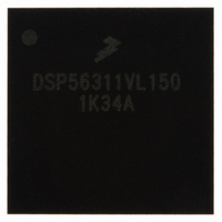
DSP56311VL150 Freescale Semiconductor, DSP56311VL150 Datasheet - Page 34

DSP56311VL150
Manufacturer Part Number
DSP56311VL150
Description
IC DSP 24BIT FIXED POINT 196-BGA
Manufacturer
Freescale Semiconductor
Series
DSP563xxr
Type
Fixed Pointr
Datasheet
1.DSP56311VL150R2.pdf
(96 pages)
Specifications of DSP56311VL150
Interface
Host Interface, SSI, SCI
Clock Rate
150MHz
Non-volatile Memory
ROM (576 B)
On-chip Ram
384kB
Voltage - I/o
3.30V
Voltage - Core
1.80V
Operating Temperature
-40°C ~ 100°C
Mounting Type
Surface Mount
Package / Case
196-MAPBGA
Package
196MA-BGA
Numeric And Arithmetic Format
Fixed-Point
Maximum Speed
150 MHz
Ram Size
384 KB
Device Million Instructions Per Second
150 MIPS
Lead Free Status / RoHS Status
Lead free / RoHS Compliant
Available stocks
Company
Part Number
Manufacturer
Quantity
Price
Company:
Part Number:
DSP56311VL150
Manufacturer:
FREESCALE
Quantity:
201
Company:
Part Number:
DSP56311VL150
Manufacturer:
MOTOLOLA
Quantity:
1 045
Company:
Part Number:
DSP56311VL150
Manufacturer:
Freescale Semiconductor
Quantity:
10 000
Part Number:
DSP56311VL150
Manufacturer:
FREESCALE
Quantity:
20 000
Company:
Part Number:
DSP56311VL150B1
Manufacturer:
ST
Quantity:
101
Company:
Part Number:
DSP56311VL150B1
Manufacturer:
Freescale Semiconductor
Quantity:
10 000
Company:
Part Number:
DSP56311VL150R2
Manufacturer:
Freescale Semiconductor
Quantity:
10 000
Specifications
2.4.5.2 DRAM Timing
The selection guides in Figure 2-12 and Figure 2-15 are for primary selection only. Final selection should be based
on the timing in the following tables. For example, the selection guide suggests that four wait states must be used
for 100 MHz operation with Page Mode DRAM. However, consulting the appropriate table, a designer can evaluate
whether fewer wait states might suffice by determining which timing prevents operation at 100 MHz, running the
chip at a slightly lower frequency (for example, 95 MHz), using faster DRAM (if it becomes available), and
manipulating control factors such as capacitive and resistive load to improve overall system performance.
2-14
No.
131
132
133
Page mode cycle time for two consecutive accesses of the same
direction
Page mode cycle time for mixed (read and write) accesses
CAS assertion to data valid (read)
Column address valid to data valid (read)
DRAM type
(tRAC ns)
100
Table 2-9.
80
70
60
Figure 2-12.
50
Characteristics
1 Wait states
2 Wait states
40
DRAM Page Mode Timings, Three Wait States
DSP56311 Technical Data, Rev. 8
DRAM Page Mode Wait State Selection Guide
Note:
66
This figure should be used for primary selection. For exact
and detailed timings, see the following tables.
80
Symbol
t
t
CAC
t
100
PC
AA
3 Wait states
4 Wait states
120
Expression
2 × T
3 × T
3.5 × T
4 × T
Chip frequency
(MHz)
C
C
− 5.7
− 5.7
C
C
1,2,3
4
Freescale Semiconductor
Min
40.0
35.0
—
—
100 MHz
Max
14.3
24.3
—
—
Unit
ns
ns
ns
ns


