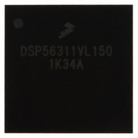
DSP56311VL150 Freescale Semiconductor, DSP56311VL150 Datasheet - Page 35

DSP56311VL150
Manufacturer Part Number
DSP56311VL150
Description
IC DSP 24BIT FIXED POINT 196-BGA
Manufacturer
Freescale Semiconductor
Series
DSP563xxr
Type
Fixed Pointr
Datasheet
1.DSP56311VL150R2.pdf
(96 pages)
Specifications of DSP56311VL150
Interface
Host Interface, SSI, SCI
Clock Rate
150MHz
Non-volatile Memory
ROM (576 B)
On-chip Ram
384kB
Voltage - I/o
3.30V
Voltage - Core
1.80V
Operating Temperature
-40°C ~ 100°C
Mounting Type
Surface Mount
Package / Case
196-MAPBGA
Package
196MA-BGA
Numeric And Arithmetic Format
Fixed-Point
Maximum Speed
150 MHz
Ram Size
384 KB
Device Million Instructions Per Second
150 MIPS
Lead Free Status / RoHS Status
Lead free / RoHS Compliant
Available stocks
Company
Part Number
Manufacturer
Quantity
Price
Company:
Part Number:
DSP56311VL150
Manufacturer:
FREESCALE
Quantity:
201
Company:
Part Number:
DSP56311VL150
Manufacturer:
MOTOLOLA
Quantity:
1 045
Company:
Part Number:
DSP56311VL150
Manufacturer:
Freescale Semiconductor
Quantity:
10 000
Part Number:
DSP56311VL150
Manufacturer:
FREESCALE
Quantity:
20 000
Company:
Part Number:
DSP56311VL150B1
Manufacturer:
ST
Quantity:
101
Company:
Part Number:
DSP56311VL150B1
Manufacturer:
Freescale Semiconductor
Quantity:
10 000
Company:
Part Number:
DSP56311VL150R2
Manufacturer:
Freescale Semiconductor
Quantity:
10 000
Freescale Semiconductor
Notes:
No.
134
135
136
137
138
139
140
141
142
143
144
145
146
147
148
149
150
151
152
153
154
155
156
CAS deassertion to data not valid (read hold time)
Last CAS assertion to RAS deassertion
Previous CAS deassertion to RAS deassertion
CAS assertion pulse width
Last CAS deassertion to RAS assertion
•
•
•
CAS deassertion pulse width
Column address valid to CAS assertion
CAS assertion to column address not valid
Last column address valid to RAS deassertion
WR deassertion to CAS assertion
CAS deassertion to WR assertion
CAS assertion to WR deassertion
WR assertion pulse width
Last WR assertion to RAS deassertion
WR assertion to CAS deassertion
Data valid to CAS assertion (write)
CAS assertion to data not valid (write)
WR assertion to CAS assertion
Last RD assertion to RAS deassertion
RD assertion to data valid
RD deassertion to data not valid
WR assertion to data active
WR deassertion to data high impedance
1.
2.
3.
4.
5.
6.
BRW[1–0] = 00, 01—not applicable
BRW[1–0] = 10
BRW[1–0] = 11
The number of wait states for Page mode access is specified in the DRAM Control Register.
The refresh period is specified in the DRAM Control Register.
The asynchronous delays specified in the expressions are valid for the DSP56311.
All the timings are calculated for the worst case. Some of the timings are better for specific cases (for example, t
T
maximum value listed, as appropriate.
BRW[1–0] (DRAM control register bits) defines the number of wait states that should be inserted in each DRAM out-of page-
access.
RD deassertion always occurs after CAS deassertion; therefore, the restricted timing is t
C
for read-after-read or write-after-write sequences). An expression is used to compute the number listed as the minimum or
Table 2-9.
Characteristics
DRAM Page Mode Timings, Three Wait States
6
5
DSP56311 Technical Data, Rev. 8
Symbol
t
t
t
t
t
t
t
RHCP
t
t
t
t
t
t
t
t
WCH
RCH
t
RWL
CWL
WCS
ROH
OFF
RSH
CAS
CRP
t
ASC
CAH
RAL
RCS
t
t
t
t
WP
DH
GA
CP
DS
GZ
0.75 × T
4.75 × T
6.75 × T
1.25 × T
0.75 × T
2.25 × T
3.75 × T
3.25 × T
1.25 × T
Expression
0.5 × T
2.5 × T
4.5 × T
1.5 × T
2.5 × T
3.5 × T
2.5 × T
3.5 × T
2.5 × T
2 × T
4 × T
1,2,3
0.25 × T
T
C
—
− 4.0
C
C
C
C
C
C
C
C
C
C
C
C
OFF
C
C
C
C
C
C
C
C
− 4.0
− 4.0
(Continued)
– 4.5
− 4.0
− 4.0
− 4.0
− 4.0
− 4.5
− 4.0
− 4.0
− 5.7
– 1.5
− 6.0
− 6.0
− 4.0
− 4.2
− 4.3
− 4.3
− 4.3
− 4.0
C
AC Electrical Characteristics
and not t
4
GZ
Min
21.0
41.0
16.0
41.5
61.5
11.0
21.0
36.0
18.3
30.5
33.2
28.2
21.0
31.0
0.0
6.0
8.5
3.5
0.5
8.2
0.0
6.0
—
—
—
.
100 MHz
PC
Max
19.3
2.5
—
—
—
—
—
—
—
—
—
—
—
—
—
—
—
—
—
—
—
—
—
—
—
equals 4 ×
Unit
ns
ns
ns
ns
ns
ns
ns
ns
ns
ns
ns
ns
ns
ns
ns
ns
ns
ns
ns
ns
ns
ns
ns
ns
2-15
—


