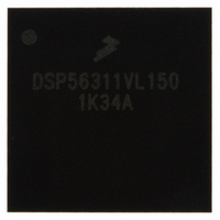
DSP56311VL150 Freescale Semiconductor, DSP56311VL150 Datasheet - Page 52

DSP56311VL150
Manufacturer Part Number
DSP56311VL150
Description
IC DSP 24BIT FIXED POINT 196-BGA
Manufacturer
Freescale Semiconductor
Series
DSP563xxr
Type
Fixed Pointr
Datasheet
1.DSP56311VL150R2.pdf
(96 pages)
Specifications of DSP56311VL150
Interface
Host Interface, SSI, SCI
Clock Rate
150MHz
Non-volatile Memory
ROM (576 B)
On-chip Ram
384kB
Voltage - I/o
3.30V
Voltage - Core
1.80V
Operating Temperature
-40°C ~ 100°C
Mounting Type
Surface Mount
Package / Case
196-MAPBGA
Package
196MA-BGA
Numeric And Arithmetic Format
Fixed-Point
Maximum Speed
150 MHz
Ram Size
384 KB
Device Million Instructions Per Second
150 MIPS
Lead Free Status / RoHS Status
Lead free / RoHS Compliant
Available stocks
Company
Part Number
Manufacturer
Quantity
Price
Company:
Part Number:
DSP56311VL150
Manufacturer:
FREESCALE
Quantity:
201
Company:
Part Number:
DSP56311VL150
Manufacturer:
MOTOLOLA
Quantity:
1 045
Company:
Part Number:
DSP56311VL150
Manufacturer:
Freescale Semiconductor
Quantity:
10 000
Part Number:
DSP56311VL150
Manufacturer:
FREESCALE
Quantity:
20 000
Company:
Part Number:
DSP56311VL150B1
Manufacturer:
ST
Quantity:
101
Company:
Part Number:
DSP56311VL150B1
Manufacturer:
Freescale Semiconductor
Quantity:
10 000
Company:
Part Number:
DSP56311VL150R2
Manufacturer:
Freescale Semiconductor
Quantity:
10 000
Specifications
2.4.8
2-32
No.
430
431
432
433
434
435
436
437
438
439
440
441
442
443
444
445
446
447
448
449
450
Clock cycle
Clock high period
•
•
Clock low period
•
•
RXC rising edge to FSR out (bit-length) high
RXC rising edge to FSR out (bit-length) low
RXC rising edge to FSR out (word-length-relative) high
RXC rising edge to FSR out (word-length-relative) low
RXC rising edge to FSR out (word-length) high
RXC rising edge to FSR out (word-length) low
Data in set-up time before RXC (SCK in Synchronous mode)
falling edge
Data in hold time after RXC falling edge
FSR input (bl, wr)
FSR input (wl)
FSR input hold time after RXC falling edge
Flags input set-up before RXC falling edge
Flags input hold time after RXC falling edge
TXC rising edge to FST out (bit-length) high
TXC rising edge to FST out (bit-length) low
TXC rising edge to FST out (word-length-relative) high
TXC rising edge to FST out (word-length-relative) low
TXC rising edge to FST out (word-length) high
For internal clock
For external clock
For internal clock
For external clock
ESSI0/ESSI1 Timing
1
6
high before RXC falling edge
6
high before RXC falling edge
Characteristics
4, 6
DSP56311 Technical Data, Rev. 8
Table 2-16.
2
2
2
2
2
ESSI Timings
Symbol
t
SSICC
Expression
4 × T
4 × T
6 × T
8 × T
3 × T
3 × T
C
C
− 10.0
− 10.0
C
C
C
C
10.0
Min
40.0
53.4
16.7
20.0
16.7
20.0
19.0
23.0
23.0
19.0
3.5
5.5
5.0
3.0
1.0
3.0
0.0
6.0
0.0
—
—
—
—
—
—
—
—
—
—
—
—
—
—
—
—
—
—
—
—
—
—
150 MHz
Freescale Semiconductor
Max
37.0
37.0
37.0
22.0
37.0
22.0
39.0
39.0
36.0
21.0
37.0
22.0
29.0
15.0
31.0
17.0
31.0
17.0
33.0
19.0
30.0
16.0
—
—
—
—
—
—
—
—
—
—
—
—
—
—
—
—
—
—
—
—
Cond-
ition
i ck a
i ck a
i ck a
i ck a
i ck a
i ck a
i ck a
i ck a
i ck a
i ck s
i ck s
x ck
x ck
x ck
x ck
x ck
x ck
x ck
x ck
x ck
x ck
x ck
x ck
x ck
x ck
x ck
x ck
x ck
x ck
x ck
i ck
i ck
i ck
i ck
i ck
i ck
i ck
i ck
5
Unit
ns
ns
ns
ns
ns
ns
ns
ns
ns
ns
ns
ns
ns
ns
ns
ns
ns
ns
ns
ns
ns
ns
ns
ns


