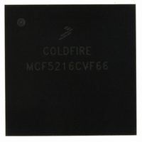
MCF5216CVF66 Freescale Semiconductor, MCF5216CVF66 Datasheet - Page 266

MCF5216CVF66
Manufacturer Part Number
MCF5216CVF66
Description
IC MPU 32BIT COLDF 256-MAPBGA
Manufacturer
Freescale Semiconductor
Series
MCF521xr
Datasheet
1.MCF5216CVM66J.pdf
(766 pages)
Specifications of MCF5216CVF66
Core Processor
Coldfire V2
Core Size
32-Bit
Speed
66MHz
Connectivity
CAN, EBI/EMI, I²C, SPI, UART/USART
Peripherals
DMA, LVD, POR, PWM, WDT
Number Of I /o
142
Program Memory Size
512KB (512K x 8)
Program Memory Type
FLASH
Ram Size
64K x 8
Voltage - Supply (vcc/vdd)
2.7 V ~ 3.6 V
Data Converters
A/D 8x12b
Oscillator Type
Internal
Operating Temperature
-40°C ~ 85°C
Package / Case
256-MAPBGA
Controller Family/series
ColdFire
Ram Memory Size
64KB
Embedded Interface Type
CAN, I2C, SPI, UART
No. Of Pwm Channels
8
Operating Temperature Range
-40°C To +85°C
No. Of Pins
256
Rohs Compliant
No
Package
256MA-BGA
Device Core
ColdFire
Family Name
MCF521x
Maximum Speed
66 MHz
Operating Supply Voltage
3.3 V
Data Bus Width
32 Bit
Number Of Programmable I/os
142
Interface Type
QSPI/UART/I2C/CAN
On-chip Adc
8-chx10-bit
Number Of Timers
8
Lead Free Status / RoHS Status
Contains lead / RoHS non-compliant
Eeprom Size
-
Available stocks
Company
Part Number
Manufacturer
Quantity
Price
Company:
Part Number:
MCF5216CVF66
Manufacturer:
FSC
Quantity:
1 670
Company:
Part Number:
MCF5216CVF66
Manufacturer:
Freescale Semiconductor
Quantity:
10 000
Part Number:
MCF5216CVF66
Manufacturer:
FREESCALE
Quantity:
20 000
Company:
Part Number:
MCF5216CVF66J
Manufacturer:
Freescale Semiconductor
Quantity:
10 000
- Current page: 266 of 766
- Download datasheet (9Mb)
Signal Descriptions
2
14.2.9
I
C Signals
2
The I
C module acts as a two-wire, bidirectional serial interface between the processor and peripherals
2
with an I
C interface (such as LCD controller, A-to-D converter, or D-to-A converter). Devices connected
2
to the I
C must have open-drain or open-collector outputs.
14.2.9.1 Serial Clock (SCL)
2
2
This bidirectional open-drain signal is the clock signal for the I
C interface. Either it is driven by the I
C
2
module when the bus is in the master mode or it becomes the clock input when the I
C is in the slave mode.
This pin can also be configured as GPIO PAS0 or UTXD2.
14.2.9.2 Serial Data (SDA)
2
This bidirectional open-drain signal is the data input/output for the I
C interface.
This pin can also be configured as GPIO PAS1 or URXD2.
14.2.10 UART Module Signals
The signals in the following sections are used to transfer serial data between three UART modules and
external peripherals.
14.2.10.1 Transmit Serial Data Output (UTXD[2:0])
UTXD[2:0] are the transmitter serial data outputs for the UART modules. The output is held high (mark
condition) when the transmitter is disabled, idle, or in the local loopback mode. Data is shifted out, lsb
first, on this pin at the falling edge of the serial clock source.
The UTXD[1:0] pins can be configured as GPIO ports PUA2 and PUA0. The UTXD2 output is offered on
3 pins and is a secondary function of the EMDC/ GPIO port PAS4 pin, CANTX/GPIO port PAS2 pin, and
SCL/GPIO port PAS0 pin.
14.2.10.2 Receive Serial Data Input (URXD[2:0])
URXD[2:0] are the receiver serial data inputs for the UART modules. Data received on these pins is
sampled on the rising edge of the serial clock source lsb first. When the UART clock is stopped for
power-down mode, any transition on this pin restarts it.
The URXD[1:0] pins can be configured as GPIO ports PUA3 and PUA1. The URXD2 input is offered on
3 pins and is a secondary function of the EMDIO/GPIO port PAS5 pin, CANRX/GPIO port PAS3 pin, and
SDA/GPIO port PAS1 pin.
14.2.10.3 Clear-to-Send (UCTS[1:0])
The UCTS[1:0] signals are the clear-to-send (CTS) inputs, indicating to the UART modules that they can
begin data transmission.
The UCTS[1:0] inputs are each offered as secondary functions on four pins--DTIN2, DTOUT2, DTIN0
and DTOUT0.
MCF5282 and MCF5216 ColdFire Microcontroller User’s Manual, Rev. 3
14-26
Freescale Semiconductor
Related parts for MCF5216CVF66
Image
Part Number
Description
Manufacturer
Datasheet
Request
R
Part Number:
Description:
Manufacturer:
Freescale Semiconductor, Inc
Datasheet:
Part Number:
Description:
Manufacturer:
Freescale Semiconductor, Inc
Datasheet:
Part Number:
Description:
Manufacturer:
Freescale Semiconductor, Inc
Datasheet:
Part Number:
Description:
Manufacturer:
Freescale Semiconductor, Inc
Datasheet:
Part Number:
Description:
Manufacturer:
Freescale Semiconductor, Inc
Datasheet:
Part Number:
Description:
Manufacturer:
Freescale Semiconductor, Inc
Datasheet:
Part Number:
Description:
Manufacturer:
Freescale Semiconductor, Inc
Datasheet:
Part Number:
Description:
Manufacturer:
Freescale Semiconductor, Inc
Datasheet:
Part Number:
Description:
Manufacturer:
Freescale Semiconductor, Inc
Datasheet:
Part Number:
Description:
Manufacturer:
Freescale Semiconductor, Inc
Datasheet:
Part Number:
Description:
Manufacturer:
Freescale Semiconductor, Inc
Datasheet:
Part Number:
Description:
Manufacturer:
Freescale Semiconductor, Inc
Datasheet:
Part Number:
Description:
Manufacturer:
Freescale Semiconductor, Inc
Datasheet:
Part Number:
Description:
Manufacturer:
Freescale Semiconductor, Inc
Datasheet:
Part Number:
Description:
Manufacturer:
Freescale Semiconductor, Inc
Datasheet:


