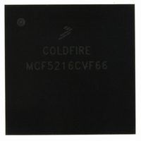
MCF5216CVF66 Freescale Semiconductor, MCF5216CVF66 Datasheet - Page 539

MCF5216CVF66
Manufacturer Part Number
MCF5216CVF66
Description
IC MPU 32BIT COLDF 256-MAPBGA
Manufacturer
Freescale Semiconductor
Series
MCF521xr
Datasheet
1.MCF5216CVM66J.pdf
(766 pages)
Specifications of MCF5216CVF66
Core Processor
Coldfire V2
Core Size
32-Bit
Speed
66MHz
Connectivity
CAN, EBI/EMI, I²C, SPI, UART/USART
Peripherals
DMA, LVD, POR, PWM, WDT
Number Of I /o
142
Program Memory Size
512KB (512K x 8)
Program Memory Type
FLASH
Ram Size
64K x 8
Voltage - Supply (vcc/vdd)
2.7 V ~ 3.6 V
Data Converters
A/D 8x12b
Oscillator Type
Internal
Operating Temperature
-40°C ~ 85°C
Package / Case
256-MAPBGA
Controller Family/series
ColdFire
Ram Memory Size
64KB
Embedded Interface Type
CAN, I2C, SPI, UART
No. Of Pwm Channels
8
Operating Temperature Range
-40°C To +85°C
No. Of Pins
256
Rohs Compliant
No
Package
256MA-BGA
Device Core
ColdFire
Family Name
MCF521x
Maximum Speed
66 MHz
Operating Supply Voltage
3.3 V
Data Bus Width
32 Bit
Number Of Programmable I/os
142
Interface Type
QSPI/UART/I2C/CAN
On-chip Adc
8-chx10-bit
Number Of Timers
8
Lead Free Status / RoHS Status
Contains lead / RoHS non-compliant
Eeprom Size
-
Available stocks
Company
Part Number
Manufacturer
Quantity
Price
Company:
Part Number:
MCF5216CVF66
Manufacturer:
FSC
Quantity:
1 670
Company:
Part Number:
MCF5216CVF66
Manufacturer:
Freescale Semiconductor
Quantity:
10 000
Part Number:
MCF5216CVF66
Manufacturer:
FREESCALE
Quantity:
20 000
Company:
Part Number:
MCF5216CVF66J
Manufacturer:
Freescale Semiconductor
Quantity:
10 000
- Current page: 539 of 766
- Download datasheet (9Mb)
Chapter 28
Queued Analog-to-Digital Converter (QADC)
The queued analog-to-digital converter (QADC) is a 10-bit, unipolar, successive approximation converter.
Up to eight analog input channels can be supported using internal multiplexing. A maximum of 18 input
channels can be supported in the expanded, externally multiplexed mode.
The QADC consists of an analog front-end and a digital control subsystem. The analog section includes
input pins, an analog multiplexer, and sample and hold analog circuits.
The digital control section contains queue control logic to sequence the conversion process and interrupt
generation logic. Also included are the periodic/interval timer, control and status registers, the conversion
command word (CCW) table, random-access memory (RAM), and the result table RAM.
The bus interface unit (BIU) provides access to registers that configure the QADC, control the
analog-to-digital converter and queue mechanism, and present formatted conversion results.
28.1
Features of the QADC module include:
Freescale Semiconductor
•
•
•
•
•
•
•
•
•
•
•
•
•
•
Internal sample and hold
Up to eight analog input channels using internal multiplexing
Up to four external analog multiplexers directly supported
Up to 18 total input channels with internal and external multiplexing
Programmable input sample time for various source impedances
Two conversion command word (CCW) queues with a total of 64 entries for setting conversion
parameters of each A/D conversion
Subqueues possible using pause mechanism
Queue complete and pause interrupts available on both queues
Queue pointers indicating current location for each queue
Automated queue modes initiated by:
— External edge trigger and gated trigger
— Periodic/interval timer, within QADC module (queues 1 and 2)
— Software command
Single scan or continuous scan of queues
64 result registers
Output data readable in three formats:
— Right-justified unsigned
— Left-justified signed
— Left-justified unsigned
Unused analog channels can be used as discrete input/output pins.
Features
MCF5282 and MCF5216 ColdFire Microcontroller User’s Manual, Rev. 3
28-1
Related parts for MCF5216CVF66
Image
Part Number
Description
Manufacturer
Datasheet
Request
R
Part Number:
Description:
Manufacturer:
Freescale Semiconductor, Inc
Datasheet:
Part Number:
Description:
Manufacturer:
Freescale Semiconductor, Inc
Datasheet:
Part Number:
Description:
Manufacturer:
Freescale Semiconductor, Inc
Datasheet:
Part Number:
Description:
Manufacturer:
Freescale Semiconductor, Inc
Datasheet:
Part Number:
Description:
Manufacturer:
Freescale Semiconductor, Inc
Datasheet:
Part Number:
Description:
Manufacturer:
Freescale Semiconductor, Inc
Datasheet:
Part Number:
Description:
Manufacturer:
Freescale Semiconductor, Inc
Datasheet:
Part Number:
Description:
Manufacturer:
Freescale Semiconductor, Inc
Datasheet:
Part Number:
Description:
Manufacturer:
Freescale Semiconductor, Inc
Datasheet:
Part Number:
Description:
Manufacturer:
Freescale Semiconductor, Inc
Datasheet:
Part Number:
Description:
Manufacturer:
Freescale Semiconductor, Inc
Datasheet:
Part Number:
Description:
Manufacturer:
Freescale Semiconductor, Inc
Datasheet:
Part Number:
Description:
Manufacturer:
Freescale Semiconductor, Inc
Datasheet:
Part Number:
Description:
Manufacturer:
Freescale Semiconductor, Inc
Datasheet:
Part Number:
Description:
Manufacturer:
Freescale Semiconductor, Inc
Datasheet:


