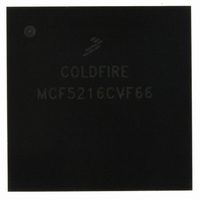
MCF5216CVF66 Freescale Semiconductor, MCF5216CVF66 Datasheet - Page 563

MCF5216CVF66
Manufacturer Part Number
MCF5216CVF66
Description
IC MPU 32BIT COLDF 256-MAPBGA
Manufacturer
Freescale Semiconductor
Series
MCF521xr
Datasheet
1.MCF5216CVM66J.pdf
(766 pages)
Specifications of MCF5216CVF66
Core Processor
Coldfire V2
Core Size
32-Bit
Speed
66MHz
Connectivity
CAN, EBI/EMI, I²C, SPI, UART/USART
Peripherals
DMA, LVD, POR, PWM, WDT
Number Of I /o
142
Program Memory Size
512KB (512K x 8)
Program Memory Type
FLASH
Ram Size
64K x 8
Voltage - Supply (vcc/vdd)
2.7 V ~ 3.6 V
Data Converters
A/D 8x12b
Oscillator Type
Internal
Operating Temperature
-40°C ~ 85°C
Package / Case
256-MAPBGA
Controller Family/series
ColdFire
Ram Memory Size
64KB
Embedded Interface Type
CAN, I2C, SPI, UART
No. Of Pwm Channels
8
Operating Temperature Range
-40°C To +85°C
No. Of Pins
256
Rohs Compliant
No
Package
256MA-BGA
Device Core
ColdFire
Family Name
MCF521x
Maximum Speed
66 MHz
Operating Supply Voltage
3.3 V
Data Bus Width
32 Bit
Number Of Programmable I/os
142
Interface Type
QSPI/UART/I2C/CAN
On-chip Adc
8-chx10-bit
Number Of Timers
8
Lead Free Status / RoHS Status
Contains lead / RoHS non-compliant
Eeprom Size
-
Available stocks
Company
Part Number
Manufacturer
Quantity
Price
Company:
Part Number:
MCF5216CVF66
Manufacturer:
FSC
Quantity:
1 670
Company:
Part Number:
MCF5216CVF66
Manufacturer:
Freescale Semiconductor
Quantity:
10 000
Part Number:
MCF5216CVF66
Manufacturer:
FREESCALE
Quantity:
20 000
Company:
Part Number:
MCF5216CVF66J
Manufacturer:
Freescale Semiconductor
Quantity:
10 000
- Current page: 563 of 766
- Download datasheet (9Mb)
Freescale Semiconductor
15–10
Bit(s)
Address
7–6
5–0
9
8
Reset
R/W:
Field
IST1
Name
CHAN
7
BYP
IST
—
P
MCF5282 and MCF5216 ColdFire Microcontroller User’s Manual, Rev. 3
Figure 28-14. Conversion Command Word Table (CCW)
IST0
6
Reserved, should be cleared.
Pause. Allows subqueues to be created within queue 1 and queue 2. The QADC
performs the conversion specified by the CCW with the pause bit set and then the
queue enters the pause state. Another trigger event causes execution to continue from
the pause to the next CCW.
1 Enter pause state after execution of current CCW.
0 Do not enter pause state after execution of current CCW.
NOTE: The P bit does not cause the queue to pause in software-initiated modes or
externally gated modes.
Sample amplifier bypass. Enables the amplifier bypass mode for a conversion and
subsequently changes the timing. The initial sample time is eliminated, reducing the
potential conversion time by two QCLKs. However, due to internal RC effects, a
minimum final sample time of four QCLKs must be allowed. When using this mode,
the external circuit should be of low source impedance. Loading effects of the external
circuitry need to be considered because the benefits of the sample amplifier are not
present.
1 Amplifier bypass mode enabled
0 Amplifier bypass mode disabled
NOTE: BYP is maintained for software compatibility but has no functional benefit on
this version of the QADC.
Input sample time. Specifies the length of the sample window. The input sample time
can be varied, under software control, to accommodate various input channel source
impedances. Longer sample times permit more accurate A/D conversions of signals
with higher source impedances.
Table 28-15
The programmable sample time can also be used to adjust queue execution time or
sampling rate by increasing the time interval between conversions.
Selects the input channel number. The CCW channel field is programmed with the
channel number corresponding to the analog input signal to be sampled and
converted. The analog input signal channel number assignments and the signal
definitions vary depending on whether the QADC multiplexed or non-multiplexed
mode is used by the application. As far as queue scanning operations are concerned,
there is no distinction between an internally or externally multiplexed analog input.
Table 28-16
Table 28-17
Programming the channel field to channel 63 denotes the end of the queue. Channels
60 to 62 are special internal channels. When one of the special channels is selected,
the sampling amplifier is not used. The value of V
directly. Programming any input sample time other than two has no benefit for the
special internal channels except to lengthen the overall conversion time.
Table 28-14. CCW Field Descriptions
CHAN5
5
shows the four selectable input sample times.
shows the channel number assignments for non-multiplexed mode.
shows the channel number assignments for multiplexed mode.
IPSBAR + 0x19_0200, 0x19_027e
CHAN4
4
Undefined
R
CHAN3
Description
3
CHAN2
RL
Queued Analog-to-Digital Converter (QADC)
, V
2
RH
, or (V
CHAN1
RH
1
–V
RL
)/2 is converted
CHAN0
0
28-25
Related parts for MCF5216CVF66
Image
Part Number
Description
Manufacturer
Datasheet
Request
R
Part Number:
Description:
Manufacturer:
Freescale Semiconductor, Inc
Datasheet:
Part Number:
Description:
Manufacturer:
Freescale Semiconductor, Inc
Datasheet:
Part Number:
Description:
Manufacturer:
Freescale Semiconductor, Inc
Datasheet:
Part Number:
Description:
Manufacturer:
Freescale Semiconductor, Inc
Datasheet:
Part Number:
Description:
Manufacturer:
Freescale Semiconductor, Inc
Datasheet:
Part Number:
Description:
Manufacturer:
Freescale Semiconductor, Inc
Datasheet:
Part Number:
Description:
Manufacturer:
Freescale Semiconductor, Inc
Datasheet:
Part Number:
Description:
Manufacturer:
Freescale Semiconductor, Inc
Datasheet:
Part Number:
Description:
Manufacturer:
Freescale Semiconductor, Inc
Datasheet:
Part Number:
Description:
Manufacturer:
Freescale Semiconductor, Inc
Datasheet:
Part Number:
Description:
Manufacturer:
Freescale Semiconductor, Inc
Datasheet:
Part Number:
Description:
Manufacturer:
Freescale Semiconductor, Inc
Datasheet:
Part Number:
Description:
Manufacturer:
Freescale Semiconductor, Inc
Datasheet:
Part Number:
Description:
Manufacturer:
Freescale Semiconductor, Inc
Datasheet:
Part Number:
Description:
Manufacturer:
Freescale Semiconductor, Inc
Datasheet:


